


DMF passivating perovskite/PCBM interface for high-efficiency and stable inverted perovskite solar cells
 0
0 Abstract
A major unresolved challenge in inverted organic-inorganic hybrid perovskite solar cells (I-PSCs) is interfacial non-radiative recombination. To tackle this issue, we introduced trace dimethylformamide (tDMF) in isopropanol (tDMF/IPA) as a passivation material, carefully modifying the interface between FA0.95Cs0.05PbI3 and [6,6]-phenyl-C61-butyric acid methyl ester. The experimental results of energy dispersive X-ray spectroscopy at different voltages and angles, infrared spectroscopy, and X-ray photoelectron spectroscopy indicate that oxygen lone pair of electrons in carbonyl group (-C=O) of polar solvent N,N-dimethylformamide form coordination bonds (Pb2+ → O=C) with Pb²⁺ suspension bond on the surface of perovskite. Tafel polarization curve and dark current results reveal decrease in the charge recombination rate at the interface and decrease in leakage current, respectively, after tDMF/IPA passivation. The photoelectric conversion efficiency (PCE) of I-PSCs treated with tDMF/IPA is significantly increased from 21.44% to 23.24%, and the open-circuit voltage is also increased from 1.01 to 1.12 V. Encapsulated devices based on tDMF/IPA passivation retained over 77% of their initial PCE after being stored in ambient air for 2,736 h.

Keywords
INTRODUCTION
In the context of the global energy transition and sustainable development, perovskite solar cells (PSCs) have emerged as a transformative technology due to their exceptional photoelectric conversion efficiency (PCE), low manufacturing costs, and solution-processable fabrication. Recent advancements in materials science and interface engineering have propelled the certified PCE of PSCs to 26.7%[1], underscoring their immense potential for commercialization. Among these, inverted perovskite solar cells (I-PSCs) stand out due to their unique architecture, which enhances stability and simplifies processing compared to conventional n-i-p structures[2]. However, despite these advantages, I-PSCs face persistent challenges, including voltage losses[3], humidity-induced degradation[4], and interfacial non-radiative recombination[5], which limit their practical deployment[6].
Interface engineering has emerged as a pivotal strategy for enhancing PSC performance by synergistically regulating charge carrier dynamics at critical heterojunctions. Precise modulation of interfacial contacts between the perovskite absorber and charge transport layers (CTLs) enables threefold optimization: enhanced charge transport through minimized energy offsets[7,8], suppressed non-radiative recombination via defect passivation[9], and improved extraction efficiency by reducing interfacial resistance[10-12]. Recent advancements demonstrate the transformative potential of this approach. Perovskite films exhibit more surface defects than bulk defects. Sun et al. from Chongqing University proposed a synergistic surface engineering approach using methylammonium chloride (MACl) cooling and phenethylammonium iodide (PEAI): MACl reduces lattice strain to enhance PEAI passivation, achieving a device PCE of 25.28%[13]. To address bulk defects in FAPbI3 caused by the traditional two-step method, the team further employed low-temperature treatment (LTT) to suppress intermediate phases, improving crystallinity and charge carrier transport, resulting in a PCE of 25.43%[14]. Xiong et al. leveraged natural capsaicin as a bifunctional interface modifier, where its carboxyl groups templated epitaxial perovskite growth while conjugated π-electrons passivated Pb2+ and I- vacancies, yielding a champion device with 21.88% PCE and 83.81% fill factor (FF) alongside exceptional thermal stability[15]. In parallel, Li et al. developed a ferrocene-based derivative that established redox-active interfaces, achieving 25% efficiency with < 2% PCE loss after 1,500 h operational stability testing under AM1.5G (Air Mass 1.5 Global) illumination[16]. A breakthrough by Wang et al. used solid-phase synthesized amorphous (lysine)2PbI2 interlayers to neutralize deep-level defects through amino-Pb coordination, attaining a certified 25.94% efficiency (26.27% lab-record) with suppressed hysteresis[17]. Further progress was demonstrated by Cao et al., where 4-trifluoromethyl phenylammonium iodide (CFPA) molecules passivated CsPbI2Br surfaces via phosphonic acid anchoring, reducing trap density by 85% and boosting open-circuit voltage to 1.10 V, consequently elevating the PCE from 11.22% to 14.37% while maintaining > 90% initial performance after storage in nitrogen gas[18]. Complementing these molecular strategies, solvent engineering with N,N-dimethylformamide (DMF) plays a critical role in controlling crystallization kinetics-its strong Pb2+ coordination and aprotic nature enable dense, large-grain perovskite films with preferred orientation[19], as evidenced by 23% reduction in Urbach energy compared to dimethyl sulfoxide (DMSO)-treated counterparts[20,21]. Collectively, these interface-based strategies highlight the multiscale design principles that are essential for overcoming efficiency-stability trade-offs in next-generation photovoltaics[22,23].
Here we introduce trace dimethylformamide (tDMF) in isopropanol (tDMF/IPA) into the interface modification of FA0.95Cs0.05PbI3-based I-PSCs, exploring its potential in improving performance. To investigate changes in the properties of thin films and devices before and after tDMF/IPA passivation, we acquired energy dispersive X-ray spectroscopy at different voltages and angles, infrared spectroscopy, X-ray photoelectron spectroscopy (XPS), Mott-Schottky curves, Tafel polarization curve and dark current results, and photoelectrochemical test measurements.
EXPERIMENTAL
Formamidinium iodide (FAI, > 99.99%) was purchased from Greatcell Solar Materials Pty Ltd. (Queanbeyan, NSW, Australia). Chlorobenzene (CB, 99.8%), cesium iodide (CsI, 99.9%), DMF (99.8%), and DMSO (≥ 99.9%) were purchased from Sigma-Aldrich (Shanghai) Trading Co., Ltd. (Shanghai, China). Lead iodide (PbI2, 99.999%) and [6,6]-Phenyl C71 butyric acid methyl ester (PCBM) were purchased from Advanced Election Technology Co., Ltd. (Beijing, China). The self-assembled monolayer material [4-(3,6-dimethyl-9H-carbazol-9-yl)butyl]phosphonic acid (Me-4PACz) was obtained from TCI (Shanghai) Chemical Industry Development Co., Ltd. (Shanghai, China). Anhydrous ethanol (≥ 99.7%) was purchased from Yantai Far East Fine Chemical Co., Ltd. (Yantai, China). Isopropanol (IPA, ≥ 99.5%) was obtained from Shanghai Macklin Biochemical Technology Co., Ltd. (Shanghai, China). The electron-transport materials 2,9-dimethyl-4,7-diphenyl-1,10-phenanthroline (BCP) and patterned indium tin oxide (ITO) glass substrates were purchased from Yingkou OPVI New Energy Technology Co., Ltd. (Yingkou, China).
Synthesis of FA0.95Cs0.05PbI3: CsI (18.2 mg), FAI (228.4 mg) and PbI2 (645.4 mg) were dissolved in a mixed solvent of DMF and DMSO (4:1 volume ratio), and stirred overnight in an N2 glove box at room temperature to prepare a 1.5 M perovskite precursor solution.
Fabrication and Characterizations of ITO/NiOx/Me-4PACz/FA0.95Cs0.05PbI3/PCBM/ BCP/Ag Devices: The ITO glass was sequentially sonicated in glass cleaning solution, water, and ethanol, followed by ultraviolet (UV)-ozone treatment for 10 min, and then rinsed again. An aqueous NiOx solution (20 mg/mL) was spin-coated on the ITO glass at 3,000 revolutions per minute (rpm) for 60 s. The Me-4PACz ethanol solution (0.5 mg/mL) was subsequently spin-coated on the NiOx film at 3,000 rpm for 30 s, followed by annealing on a hot plate at 100 °C for 10 min. Seventy microliters of perovskite precursor were spin-coated on the Me-4PACz substrate using a two-step procedure: 1,500 rpm for 10 s, then 4,000 rpm for 40 s. During the second step, 200 μL of CB was added at the 34th second. The films were then annealed at 100 °C for 30 min. For the DMF-FA0.95Cs0.05PbI3 preparation, a DMF/IPA solution (7.70 mg/mL) was dynamically spin-coated onto the perovskite film [Supplementary Figure 1]. A PCBM CB solution (20 mg/mL) was spin-coated onto the perovskite at 2,500 rpm for 40 s, followed by a BCP saturated solution (0.5 mg/mL) at 5,000 rpm for 30 s. Finally, Ag electrodes were deposited by thermal evaporation.
Materials characterization. The X-Ray Diffraction (XRD) patterns of perovskite films were recorded using a high-resolution diffractometer (SmartLab 9 kW, Rigaku, Japan) equipped with a two-dimensional (2D) matrix high-speed detector at 45 kV, 200 mA, with Cu Kα (λ = 1.54 Å) as the radiation source, from 5° to 80° (scan step 0.01°, scan rate 20°/min). The morphology of the perovskite films was examined by focused ion beam scanning electron microscopy (FIB-SEM) using a Thermo Fisher Scientific GX4 instrument (USA) at 10 kV, 43 pA emitter current, and a 4.5 mm working distance. The elemental content and distribution of the perovskite films were determined by energy dispersive spectroscopy (EDS, Bruker, Billerica, MA, USA) coupled with scanning electron microscopy (SEM). The detected X-rays were excited by an electron beam of 10 kV and 43 pA. XPS and UPS were used to analyze the thin films, with UPS employing helium Iα radiation (21.22 eV) as the excitation source. The three-dimensional morphology was measured by atomic force microscopy (AFM, Bruker, Billerica, MA, USA). The absorbance and transmittance of the films were measured using a 500 UV-visible (UV-Vis) spectrophotometer (Shimadzu, Kyoto, Japan) over a wavelength range of 300-900 nm. Time-resolved photoluminescence (TRPL) was recorded with a FLS1000 photoluminescence spectrometer (Tianmei Instruments Ltd., Beijing, China). Fourier transform infrared (FTIR) spectroscopy was performed with a Thermo Fisher iS50 (Waltham, MA, USA).
The linear sweep voltammetry (LSV) of PSCs-ITO-high-transparency glass at zero light intensity was measured using a ZAHNER cmps-2 Pro optoelectronic workstation (ZAHNER, Germany). The scan rate was 100 mVs-1, and the scan range was -1.5 to 1.5 V (absolute). The photovoltaic characteristics of the devices were measured with a solar simulator (AAA class) at a power density of 100 mW cm-2. The incident photon-to-current efficiency (IPCE) of MCP ITO-IEs at 80% light intensity was recorded using a photoelectrochemical workstation over different wavelengths.
Grazing-incidence wide-angle X-ray scattering (GIWAXS) data of the perovskite films were collected on the BL17B1 beamline of the National Facility for Protein Science in Shanghai (NFPS) at the Shanghai Synchrotron Radiation Facility (SSRF, Shanghai, China). The beamline is equipped with a PILATUS3 S-2M detector for GIWAXS measurements. Measurements were performed using 10 keV X-rays at an incidence angle of 0.2°, with an exposure time of 3 s per sample, allowing characterization of both the surface and bulk of the perovskite films. The resulting spectra were processed and analyzed using the software packages Athena and Artemis.
RESULTS AND DISCUSSION
The concentration of DMF in IPA should be kept low, as DMF is a solvent capable of dissolving perovskites; a small amount does not disrupt the bulk structure. To determine whether the optimized DMF concentration (7.70 mg/mL) alters the bulk structure of FA0.95Cs0.05PbI3 perovskite films, XRD patterns were collected for films treated with tDMF/IPA passivation, using untreated films as a control. As shown in Supplementary Figure 2, no new PbI2 peaks were observed in the tDMF/IPA-passivated films. After passivation with tDMF/IPA, the full width at half maximum (FWHM) of the (100) peak (approximately 0.085° vs. about 0.096° in the control group) and the (110) peak (approximately 0.099° vs. about 0.105° in the control group) slightly decreased [Supplementary Figure 3], confirming that tDMF/IPA does not disrupt the bulk crystal structure and even slightly improves crystallinity.
The core of this work lies in elucidating the synergistic effect between DMF and Pb2+: the specific coordination interaction between the carbonyl group (-C=O) in DMF molecules and the uncoordinated Pb2+ dangling bonds on the surface of FA0.95Cs0.05PbI3 perovskite. Specifically, the oxygen atom of the carbonyl group acts as a Lewis base, donating its lone pair of electrons to the empty orbitals of Pbb2+, forming a stable Pb-O coordination bond (Pb2+ ← O=C). This process suppresses surface defects through two mechanisms: on one hand, the coordination saturates the dangling bonds on the Pb2+ surface, reducing energy level defects caused by uncoordinated sites; on the other hand, a small amount of DMF molecules can replace the iodide ions on the perovskite surface to coordinate with Pb2+, further optimizing the surface chemical environment and thereby inhibiting defect formation. Ingmar Persson also confirmed the coordination mechanism of Pb2+ with DMF carbonyl oxygen (C=O)[24]. To investigate the effect of tDMF/IPA passivation on the film surface, we performed GIWAXS tests, and the 2D diffraction patterns are shown in Figure 1A and B. In the 2D GIWAXS images of both types of films, clear ring patterns are observed, indicating that the film surfaces are isotropic. There are two bright spots in the 45-degree direction of the Pxy-Pz axis, corresponding to the (100) and (111) grain planes. The diffraction peak intensity of the perovskite film processed by tDMF/IPA is slightly enhanced at scattering vector q values of 0.95 Å-1 and 1.87 Å-1. The radial integration intensity of the GIWAXS pattern, as shown in Figure 1C, changes at 2.0 Å-1 after DMF passivation treatment. These results collectively show that there are some alterations in the diffraction of the perovskite film surface after tDMF/IPA treatment.
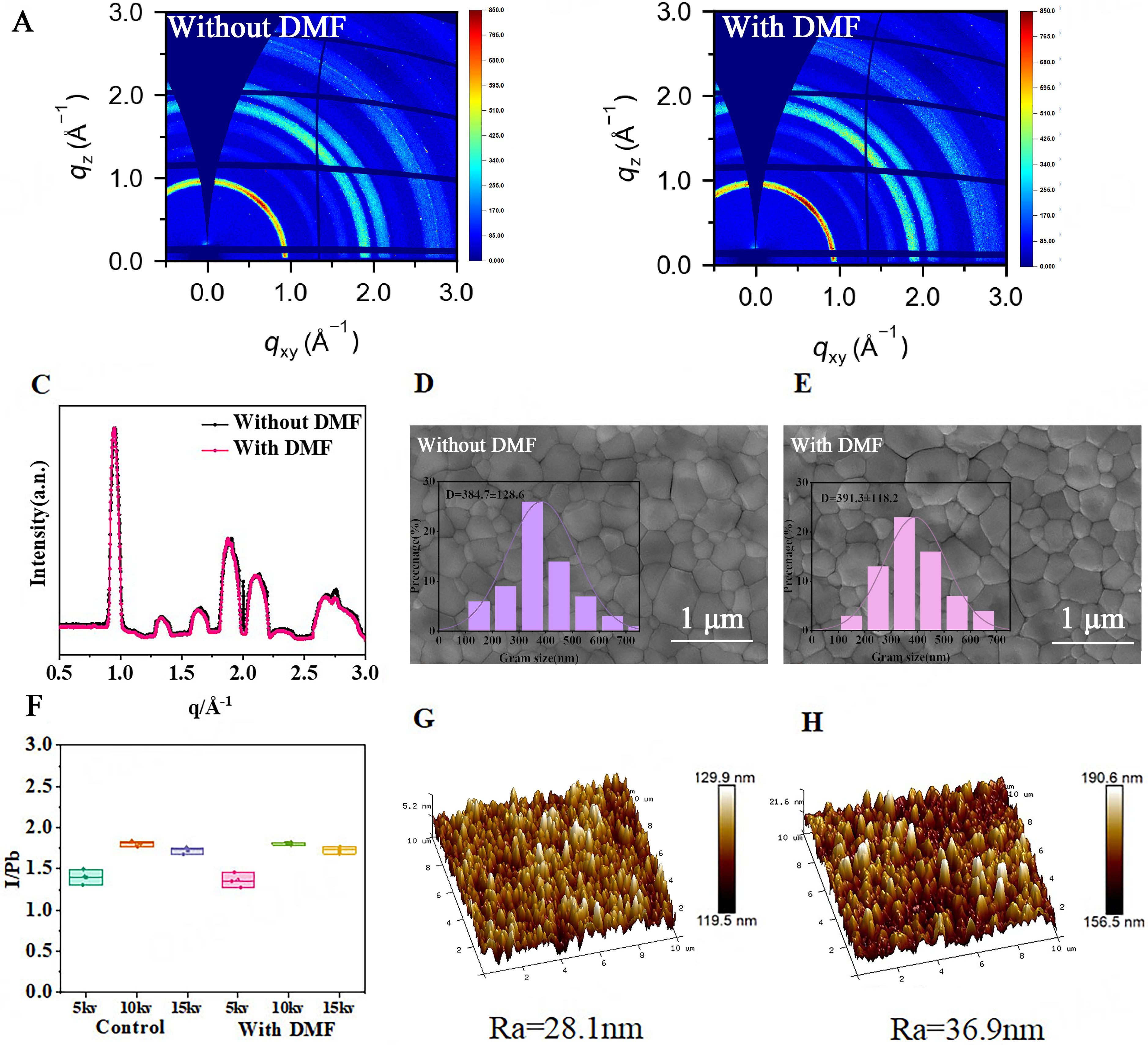
Figure 1. GIWAXS of perovskite films before (A) and after (B) DMF passivation; (C) GIWAXS intensity integration curves of perovskite film crystallization; SEM images before (D) and after (E) passivation; (F) EDS spectra of the I/Pb ratio in FA0.95Cs0.05PbI3 perovskite films at different energies before and after passivation; AFM images before (G) and after (H) passivation. DMF: N,N-dimethylformamide; Ra: surface roughness; GIWAXS: grazing-incidence wide-angle X-ray scattering; EDS: energy dispersive spectroscopy.
SEM was used to image the surface topography of the films before and after passivation. The SEM images clearly show the size of the perovskite grains (Figure 1D and E; statistical distribution in the inset), with the average grain size of the control film being 384 nm. The average grain size of the film after tDMF/IPA treatment was 391 nm, indicating no significant difference in grain size before and after passivation. Compared to the perovskite film surface before passivation, the grains after tDMF/IPA passivation exhibit a three-dimensional appearance. As shown in Supplementary Figure 4, the enlarged SEM image reveals more distinct boundaries between the perovskite grains. The vertical features, however, are difficult to characterize due to the limitations of SEM in observing changes along the Z-axis.
To study changes in elemental content on the film surface before and after passivation, EDS measurements were performed at different voltages and angles. The EDS results at different voltages are shown in Figure 1F. Compared with the unpassivated film, the I/Pb ratio after passivation did not change significantly at 10 and 15 kV. At a lower voltage of 5 kV, however, the I/Pb ratio of the passivated surface decreased. EDS probes elements within a 1-5 μm depth range in SEM, and lower applied voltages correspond to shallower sampling depths, making the results more sensitive to the surface composition. The reduction of the surface I/Pb ratio after passivation indicates that some surface iodine is replaced by DMF via carbonyl-Pb2+ coordination. To further investigate surface elemental changes, the angle between the incident electron beam and the film surface was reduced from 90° to 65° to enhance the surface signal. After passivation, the I/Pb ratio also decreased with decreasing angle [Supplementary Figure 5]. This behavior is attributed to coordination between Pb2+ and the carbonyl group (C=O) of DMF. The carbonyl oxygen of DMF, acting as a strong Lewis base, preferentially coordinates with high-density Pb2+ dangling bonds on the surface. These results demonstrate that DMF effectively regulates surface element redistribution through coordination, compensates for iodine vacancy defects, and optimizes the surface chemical environment of the film.
To explore the microscopic structure of the film surface more accurately, AFM, which is highly sensitive to surface features, was employed for in-depth characterization. As shown in the AFM images [Figure 1G and H], the surface roughness (Ra) of the film before passivation was 28.1 nm, while after tDMF/IPA passivation it increased to 36.9 nm. This comparison indicates that tDMF/IPA treatment increases the nanoscale roughness of the perovskite film surface, thereby enhancing the contact area between the perovskite layer and the PCBM layer.
XPS was used to detect changes in lead (Pb) elements and their chemical states in the films before and after tDMF/IPA passivation [Figure 2A]. By analyzing the XPS curve of Pb 4f, the peaks of Pb 4f7/2 and Pb 4f5/2 in the tDMF/IPA-modified thin film are located at 138.0 and 142.9 eV, respectively, and they move towards higher binding energies compared to the binding energies of the control thin film (137.9 and 142.8 eV) and show higher energy values. After the tDMF/IPA passivation treatment, DMF interacts with the Pb²⁺ on the perovskite surface, leading to a decrease in the electron cloud density around the Pb atoms and an increase in the effective nuclear charge, thereby enhancing the binding energy.
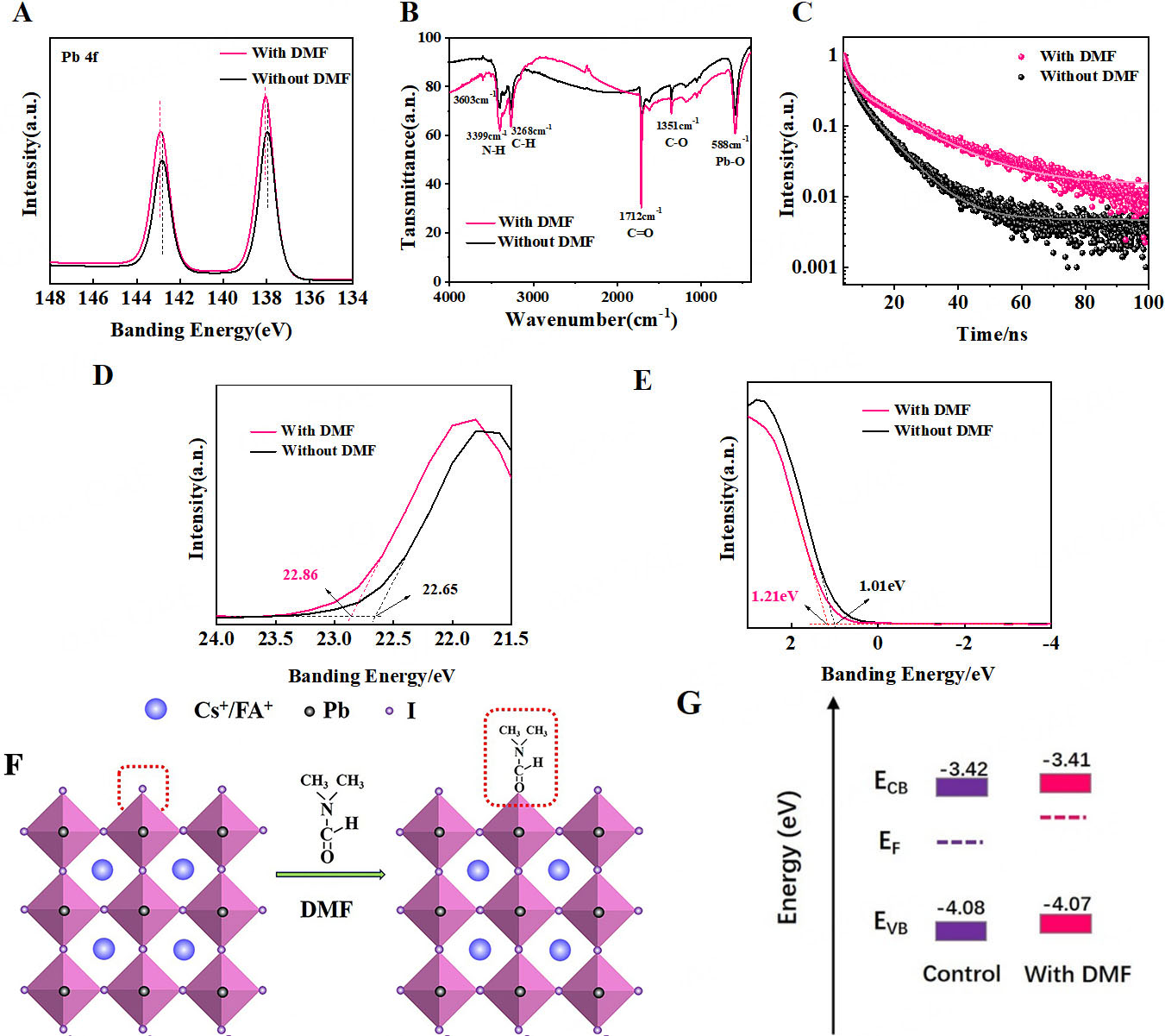
Figure 2. XPS energy spectra of FA0.95Cs0.05PbI3 perovskite thin films before and after DMF passivation. High resolution (A) Pb 4f, (B) FTIR spectra of films; (C) TRPL for control and DMF-treated perovskite films; (D) UPS energy spectra of secondary electron cutoff region and (E) Fermi energy cutoff region; (F) Interaction diagram between DMF and FA0.95Cs0.05PbI3; (G) Energy level diagram of perovskite films before and after DMF passivation. DMF: N,N-dimethylformamide; ECB: conduction band energy; EF: Fermi energy; EVB: valence band energy; XPS: X-ray photoelectron spectroscopy; FTIR: Fourier transform infrared; TRPL: time-resolved photoluminescence.
To further explore the effect of tDMF/IPA passivation on the chemical bonds on the surface of the film, FTIR was performed. Firstly, PbI2, FAI, DMF, and CsI were prepared as blank control groups, and the FTIR spectral data of the perovskite films before and after tDMF/IPA passivation were collected, as shown in Figure 2B. By comparing the spectra of the blank samples such as PbI2, FAI, DMF, and CsI in Supplementary Figure 6, the positions of the absorption peaks were determined. The enhancement of the Pb-O absorption peak at 588 cm-1 is attributed to the coordination effect between the carbonyl group in DMF and the uncoordinated Pb2+, which promotes the formation of new Pb-O-C bonds and increases the intensity of the absorption peak.
To investigate the influence of tDMF/IPA-modified perovskite/electron transport layer (PVK/ETL) interfaces on charge carrier dynamics, we performed TRPL measurements on FA0.95Cs0.05PbI3 thin films deposited onto ITO/glass substrates. As shown in Figure 2C, the average carrier lifetimes of the perovskite films before and after DMF passivation are 50 ns and 100 ns, respectively. The carrier lifetimes are obtained using the double exponential equation[25]:
where τ1 and τ2 denote the fast and slow decay times, respectively, associated with trap states, interface charge transfer processes, and free carrier recombination. The τ1 and τ2 values were obtained through double-exponential fitting of the decay curves. Before passivation, τ1 = 1.75 ns and τ2 = 8.28 ns; after passivation, τ1 = 1.75 ns and τ2 = 15.02 ns [Supplementary Table 1]. These results correspond to an increase in the average carrier lifetime from 3.9 ns to 7.5 ns, indicating a substantially prolonged excited-state lifetime. The observations suggest that tDMF/IPA treatment effectively reduces the number of Pb2+ defects.
To explain the increase in Voc, UPS measurements were performed [Figure 2D and E]. The optical bandgap of the perovskite films, estimated from the UV-Vis absorption spectra [Supplementary Figure 7], is shown in Supplementary Figure 8, with values of 1.534 eV for the untreated film and 1.530 eV for the tDMF/IPA-passivated film. The UV-Vis spectra also indicate enhanced absorption for the passivated films, reflecting improved optical properties. Although the absorption characteristics of perovskite thin films correlate with their optoelectronic performance, no quantitative relationship has been established to link film color with device efficiency. The proposed interaction mechanism of tDMF/IPA passivation on the perovskite film is illustrated in Figure 2F.
The reduction of defects at grain boundaries and surfaces after tDMF/IPA passivation is expected to reduce light scattering within the film, allowing more light to penetrate and be absorbed. Combining the bandgap calculated from UV-Vis absorption and the valence band determined by UPS, the valence band position and conduction band position of the film were calculated. The untreated film showed a maximum valence band (VBM) at -4.08 eV, and after DMF passivation at -4.07 eV, as illustrated in the schematic energy-level diagram of the perovskite film [Figure 2G]. From this diagram, it can be observed that after tDMF/IPA treatment, the positions of the valence band energy (EVB) and conduction band energy (ECB) remained essentially unchanged, but the Fermi energy (EF) moved closer to the conduction band. As the EF shifts toward ECB when defects are reduced, the electron carrier concentration increases, facilitating efficient electron transport, consistent with the observed improvement in device performance[26].
To identify the contributions of DMF and IPA to device passivation, comparative experiments were conducted under the same processing conditions, treating perovskite films with either IPA alone or tDMF/IPA solution. The experimental results shown in Supplementary Figure 9 indicate that devices passivated with the tDMF/IPA solution perform significantly better than those passivated with pure IPA. Thus, DMF plays an important role in mixed solvent systems, and IPA is not the dominant factor in the passivation effect. We then optimized tDMF/IPA solution concentrations (3.35, 7.70, and 15.40 mg/mL) and, combined with an improved spin-coating process, systematically tested the statistical distribution of photovoltaic parameters at each concentration [Supplementary Figure 10]. The analysis shows that 7.70 mg/mL yields the optimal PCE. However, at 15.40 mg/mL, the PCE decreases, which is attributed to excess DMF partially dissolving the perovskite, disrupting its crystal structure and severely degrading photovoltaic performance. Based on this optimal concentration, we further explored the effects of static versus dynamic spin coating on photovoltaic performance [Supplementary Figure 11]. Dynamic spin coating significantly improves device performance, particularly by increasing Voc, while the short-circuit current density (Jsc) and FF remain relatively stable.
To visually demonstrate the passivation effect, we selected two representative devices for comparison (Figure 3A: ITO/NiOx/Me-4PACz/perovskite/passivator/ C60/BCP/Ag device structure diagram): the untreated control device and the device that underwent tDMF/IPA passivation treatment. The current-voltage (I-V) characteristic curves of both devices are shown in Figure 3B, with the following photovoltaic parameters: the control device exhibits a PCE of 21.44%, Voc of 1.01 V, Jsc of 26.34 mA/cm2, and FF of 80.08%; in contrast, the passivated device shows an increased PCE of 23.24%, Voc of 1.12 V, a slightly higher Jsc of 26.62 mA/cm2, and a slightly decreased FF of 77.73% (Supplementary Figure 12, statistics of Jsc and FF). The performance improvement of DMF-passivated devices is primarily attributed to the optimization of Voc and FF. We measured the hysteresis index (HI) of the control device as 5.52%, while the HI of the device modified with tDMF/IPA significantly decreased to 2.17% [Supplementary Figure 13]. This indicates that the introduction of DMF can effectively reduce defects, thereby alleviating the typical hysteresis effect in perovskite devices. The underlying mechanism may be related to the effective passivation of Pb2+ defects on the perovskite surface due to the introduction of DMF, which reduces non-radiative recombination at the interface with PCBM. Additionally, the IPCE was measured, as shown in Figure 3C. The results indicate that the current density of the control device is approximately 23.01 mA/cm2, while that of the passivated device is about 23.26 mA/cm², showing no significant change.
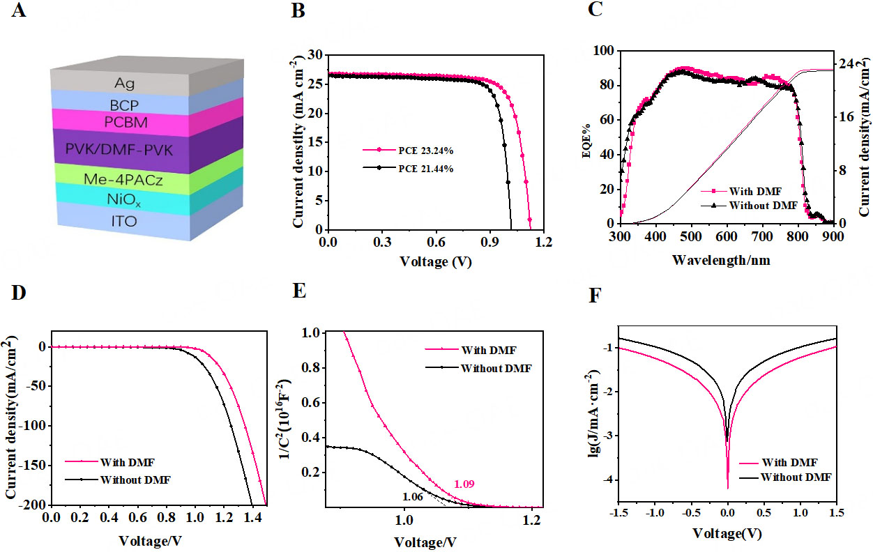
Figure 3. (A) Schematic device structure; (B) J-V curves for best-performing devices before and after DMF passivation under one solar (100 mW cm-2) light; (C) EQE spectra and integrated current densities for best-performing devices before and after DMF passivation; (D) Dark current curves; (E) Mott-Schottky curves; (F) Tafel curves. BCP: 2,9-dimethyl-4,7-diphenyl-1,10-phenanthroline; PCBM: [6,6]-Phenyl C71 butyric acid methyl ester; PVK: poly(9-vinylcarbazole); DMF: N,N-dimethylformamide; ITO: indium tin oxide; PCE: photoelectric conversion efficiency; EQE: external quantum efficiency.
The dark current of the devices was measured. As shown in Figure 3D, the curves exhibit typical semiconductor behavior. The Voc of the control device is approximately 0.9 V, while that of the passivated device increases to about 1.1 V. This reflects an increase in the parallel resistance and a reduction of short-circuit pathways between interfaces, providing a rationale for the observed voltage enhancement. Additionally, the built-in electric field of the two devices was compared using Mott-Schottky measurements [Figure 3E]. According to the Mott-Schottky equation[27]:
where:
The calculated 12 of the tDMF/IPA-passivated device (1.09 V) is higher than that of the control device (1.06 V), indicating an enhancement of approximately 30 mV in the built-in electric field. This increase in 12 suggests a reduction in carrier recombination, further confirming the positive effect of tDMF/IPA passivation on device performance. Furthermore, Tafel curves were measured to investigate the origin of the Voc increase [Figure 3F]. The results show that, compared to the control device, the polarization current and exchange current density of the passivated device decreased, indicating that passivation effectively reduces surface defects in the perovskite and lowers the electron recombination rate. In particular, the exchange current at the interface between the perovskite and the electron transport layer also decreased, contributing to a reduction in interfacial recombination.
Optical intensity-dependent measurements were performed to investigate the charge carrier recombination mechanism. The variation of Voc over a light intensity range of 10-100 mW/cm2 is shown in Supplementary Figure 14. According to common understanding, the strength of non-radiative recombination can be evaluated through the slope of the Voc versus light intensity relationship curve, which yields a value of kBT/q (where kB denotes the Boltzmann constant, T represents the temperature in Kelvin, and q signifies the elementary charge). The slope of the passivated device (1.30 kBT/q) is lower than that of the control device (1.65 kBT/q), indicating that DMF significantly decreases the interfacial recombination rate of perovskites and PCBM.
To evaluate the surface hydrophobicity of the perovskite film after tDMF/IPA passivation, the water contact angle was measured, showing an increase from 56.2° to 65.9° [Supplementary Figure 15]. This confirms that tDMF/IPA passivation occurs through coordination of the carbonyl group with Pb2+, while the methyl group in DMF enhances the surface hydrophobicity, consistent with the improved stability of the passivated devices. Surface wettability tests with CB show, as presented in Supplementary Figure 16, that CB spreads slightly better on the passivated film, facilitating improved coverage of the PCBM electron transport layer. To further evaluate device stability, aging tests were conducted at 30 °C and 50% relative humidity. As shown in Supplementary Figure 17, after 120 h of storage, the control devices exhibited yellowing earlier than the passivated devices.
To evaluate the long-term stability of PSCs after tDMF/IPA passivation, we first measured the stability of the packaged device by storing it in ambient air at ~ 30% relative humidity and ~ 25 °C. As shown in Figure 4, the tDMF/IPA passivated device shows no significant degradation after 2,736 h of aging, and maintains more than 77% of the initial PCE.
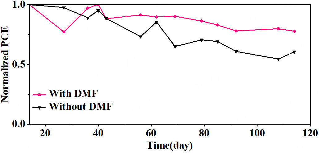
Figure 4. Normalized PCE of control group devices and DMF-treated devices packaged in air conditions for 2,736 h. PCE: Photoelectric conversion efficiency; DMF: N,N-dimethylformamide.
Given that DMSO possesses coordination ability and polarity similar to DMF, and that DMSO has been shown to coordinate more strongly with surface Pb2+ in perovskites[28], we initially applied the same procedure used for DMF, employing a tDMSO/IPA solution to passivate the perovskite/PCBM interface. Device testing before and after passivation showed an improvement in PCE [Supplementary Figure 18], indicating that DMSO is promising in interface engineering. These preliminary results lay the foundation for subsequent systematic research: we will evaluate the long-term stability of DMSO-passivated devices through accelerated aging tests, optimize the proportion and thickness of the passivation layer using a gradient concentration method, and further verify the interaction mechanism between DMSO and the perovskite surface through characterization techniques such as XPS and PL spectroscopy. These follow-up studies will deepen theoretical understanding and guide the practical application of DMSO passivation technology.
CONCLUSIONS
In summary, we successfully used tDMF/IPA as a passivation strategy to finely modify the interface between the perovskite layer and the electron transport layer, reducing defects on the perovskite surface and effectively addressing the critical issue of severe non-radiative recombination at the interface in PSCs. This strategy not only enhanced photovoltaic performance, increasing the PCE from 21.44% to 23.24%, but also facilitated efficient charge transport, significantly improving the long-term stability of the solar cell. Therefore, we propose an interface regulation strategy that provides a practical route for fabricating high-performance PSCs with broad application potential. This work deepens our understanding of perovskite interface regulation mechanisms and establishes an experimental and theoretical foundation for optimizing devices with alternative passivation strategies.
DECLARATIONS
Authors’ contributions
Conceptualization, methodology, investigation, formal analysis, visualization, writing - original draft: Shen, H.
Investigation, XRD measurements, SEM operation: Shen, H.; Wang, C.; Gao, H.
Assistance with electrochemical performance experiments: Chang, Z.
Conceptualization, supervision, funding acquisition, writing - review & editing: Zhou, H.; Zhang X.; Rosei, F.
Availability of data and materials
The data that support the findings of this study are available from the corresponding author upon reasonable request.
Financial support and sponsorship
This work was supported by the Department of Science and Technology of Shandong Province (WSR2024061) and the Department of Education of Shandong Province (SDYGJ19061, M2022083).
Conflicts of interest
Rosei, F. is an Editorial Board Member of the journal Energy Materials. Rosei, F. was not involved in any steps of the editorial process, notably including reviewers’ selection, manuscript handling, or decision-making. The other authors declare that there are no conflicts of interest.
Ethical approval and consent to participate
Not applicable.
Consent for publication
Not applicable.
Copyright
© The Author(s) 2026.
Supplementary Materials
REFERENCES
1. Wang, H.; Guerrero, A.; Bou, A.; Al-mayouf, A. M.; Bisquert, J. Kinetic and material properties of interfaces governing slow response and long timescale phenomena in perovskite solar cells. Energy. Environ. Sci. 2019, 12, 2054-79.
2. Levin, T.; Bistline, J.; Sioshansi, R.; et al. Energy storage solutions to decarbonize electricity through enhanced capacity expansion modelling. Nat. Energy. 2023, 8, 1199-208.
3. Qian, J.; He, J.; Zhang, Q.; et al. Minimizing interfacial energy losses in inverted perovskite solar cells by a dipolar stereochemical 2D perovskite interface. J. Energy. Chem. 2024, 90, 496-503.
4. Zhang, J.; Zhang, L.; Liu, J.; et al. OH spectator at IrMo intermetallic narrowing activity gap between alkaline and acidic hydrogen evolution reaction. Nat. Commun. 2022, 13, 5497.
5. Tang, H.; Shen, Z.; Shen, Y.; et al. Reinforcing self-assembly of hole transport molecules for stable inverted perovskite solar cells. Science 2024, 383, 1236-40.
6. Liu, D.; Lu, G.; Shi, B.; et al. ROS-scavenging hydrogels synergize with neural stem cells to enhance spinal cord injury repair via regulating microenvironment and facilitating nerve regeneration. Adv. Healthc. Mater. 2023, 12, e2300123.
7. Zhang, C.; Li, Y.; Yu, F.; et al. Visual growth of nano-HOFs for low‐power memristive spiking neuromorphic system. Nano. Energy. 2023, 109, 108274.
8. Othman, M.; Zhang, T.; Mcmeekin, D. P.; et al. Structural and photophysical properties of guanidinium-iodide-treated perovskite solar cells. Solar. RRL. 2022, 7, 2200852.
9. Zhang, K.; He, Y.; Guo, R.; et al. Interstitial carbon-doped PdMo bimetallene for high-performance oxygen reduction reaction. ACS. Energy. Lett. 2022, 7, 3329-36.
10. Hayashi, K. I.; Arai, K.; Aoi, Y.; et al. The main oxidative inactivation pathway of the plant hormone auxin. Nat. Commun. 2021, 12, 6752.
11. Bisquert, J. Hysteresis, impedance, and transients effects in halide perovskite solar cells and memory devices analysis by neuron-style models. Adv. Energy. Mater. 2024, 14, 2400442.
12. Chen, H.; Liu, C.; Xu, J.; et al. Improved charge extraction in inverted perovskite solar cells with dual-site-binding ligands. Science 2024, 384, 189-93.
13. Wang, C.; Ou, Z.; Pan, Y.; et al. Surface engineering of perovskite films via sequential moisture cooling and passivation for efficient solar cells. Adv. Funct. Mater. 2025, 35, 2420084.
14. Gao, Q.; Wang, C.; Pan, Y.; et al. Low-temperature purification of intermediate phases for enhanced stability and efficiency in FAPbI3 solar cells. Nano. Energy. 2025, 139, 110945.
15. Xiong, S.; Hou, Z.; Zou, S.; et al. Direct observation on p- to n-type transformation of perovskite surface region during defect passivation driving high photovoltaic efficiency. Joule 2021, 5, 467-80.
16. Li, Z.; Li, B.; Wu, X.; et al. Organometallic-functionalized interfaces for highly efficient inverted perovskite solar cells. Science 2022, 376, 416-20.
17. Wen, Y.; Zhang, T.; Wang, X.; et al. Amorphous (lysine)2PbI2 layer enhanced perovskite photovoltaics. Nat. Commun. 2024, 15, 7085.
18. Cao, S.; Wang, L.; She, X.; et al. Enhanced efficiency and stability of inverted CsPbI2Br perovskite solar cells via fluorinated organic ammonium salt surface passivation. Langmuir 2024, 40, 3715-24.
19. Zou, Y.; Yu, W.; Guo, H.; et al. A crystal capping layer for formation of black-phase FAPbI3 perovskite in humid air. Science 2024, 385, 161-7.
20. Wu, H.; Li, Z.; Zhang, F.; Kang, C.; Li, Y. Ionic liquids for efficient and stable perovskite solar cells. Adv. Mater. Inter. 2022, 9, 2201292.
21. Su, C.; Li, M. Zhang, S., et al. Multifunctional dual-crosslinked Ti3C2Tx MXene-based hydrogels for wearable sensors with enhanced mechanical robustness and broadband microwave absorption. J. Mater. Chem. A. 2025, 13, 7700-10.
22. Sun, F.; Jiang, H. Wang, H., et al. Soft fiber electronics based on semiconducting polymer. Chem. Rev. 2023, 123, 4693-763.
23. Feng, Y.; Cai, C.; Liu, B.; Yang, H.; Lee, R. Cellulose nanocrystal-incorporated mapbi3 for inverted perovskite solar cells with enhanced efficiency and stability. ACS. Appl. Energy. Mater. 2024, 7, 12092-102.
24. Persson, I.; Lyczko, K.; Lundberg, D.; Eriksson, L.; Płaczek, A. Coordination chemistry study of hydrated and solvated lead(II) ions in solution and solid state. Inorg. Chem. 2011, 50, 1058-72.
25. Chen, J.; Lv, J.; Liu, X.; Lin, J.; Chen, X. A study on theoretical models for investigating time-resolved photoluminescence in halide perovskites. Phys. Chem. Chem. Phys. 2023, 25, 7574-88.
26. You, G.; Du, K.; Zheng, Y.; et al. Orientation-tuned piperazinium derivatives for efficient and stable inverted perovskite solar cells. ACS. Appl. Mater. Interfaces. 2025, 17, 59453-61.
27. El-Khozondar, H. J.; Seriani, N.; He, T.; Xie, F. Generalized Mott–Schottky analysis of photoelectrodes. J. Phys. Chem. C. 2025, 129, 14593-7.
Cite This Article
How to Cite
Download Citation
Export Citation File:
Type of Import
Tips on Downloading Citation
Citation Manager File Format
Type of Import
Direct Import: When the Direct Import option is selected (the default state), a dialogue box will give you the option to Save or Open the downloaded citation data. Choosing Open will either launch your citation manager or give you a choice of applications with which to use the metadata. The Save option saves the file locally for later use.
Indirect Import: When the Indirect Import option is selected, the metadata is displayed and may be copied and pasted as needed.
About This Article
Special Topic
Copyright

Data & Comments
Data
0


Comments
Comments must be written in English. Spam, offensive content, impersonation, and private information will not be permitted. If any comment is reported and identified as inappropriate content by OAE staff, the comment will be removed without notice. If you have any queries or need any help, please contact us at support@oaepublish.com.