

Towards deterministic and functional atomic manufacturing with electron beams
 0
0 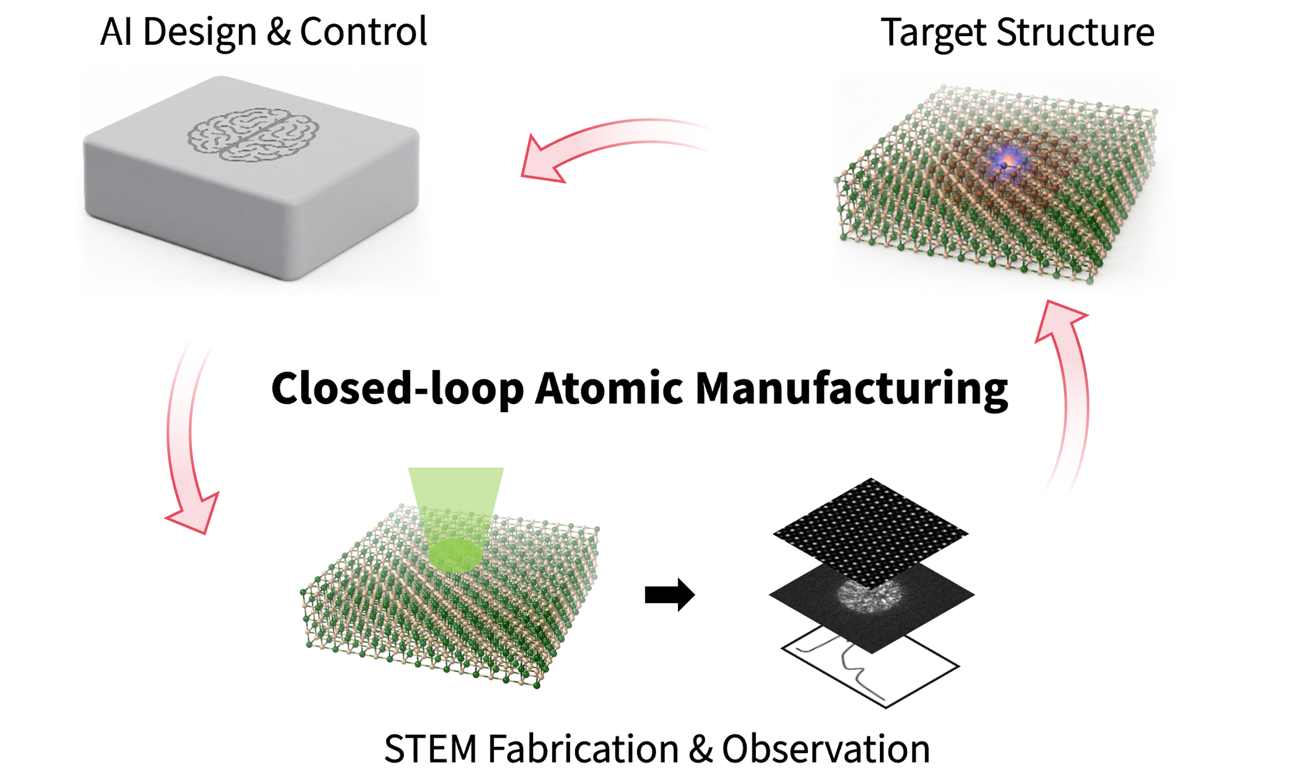


 Download PDF
Atomic-scale manipulation has long been regarded as a fundamental capability for realizing next-generation quantum devices[1-4], novel functional materials[5], and programmable matter[6]. Advances in scanning probe microscopy[7], ion implantation[8], and electron microscopy[9] have demonstrated that atoms can be displaced, assembled and transformed into artificial structures with increasing spatial precision. The concept of manipulation with atomic precision by a focused electron beam was proposed as early as 2014[10]. Among existing platforms, scanning transmission electron microscopy (STEM) offers a particularly attractive realization of this vision because its sub-angstrom focused electron probe enables localized momentum and energy transfer while simultaneously imaging structural evolution at atomic resolution[11].
Despite these promises, electron-beam-based atomic engineering remains largely exploratory. Previous demonstrations were mostly restricted to surfaces and atomically thin materials where knock-on collisions and localized radiolysis drive lattice reconstruction and defect migration. Such approaches have enabled subtractive sculpting of sub-nanometer structures[12], localized polymorphic transitions[13], and the creation of unconventional structure and chemistry[14-16]. In bulk three-dimensional (3D) solids, electron beam engineering was applied to dopant positioning and assembly[17], localized crystallization of amorphous phases[18], and patterned structural phase transitions[19,20]. These earlier works mostly relied on empirical trial-and-error, lacking a deterministic framework for predefining fabrication outcomes from beam parameters. Extending atomic manipulation into scalable manufacturing therefore remains a central challenge, requiring quantitative understanding of beam-matter interactions, programmable control of structural evolution, and preservation of structural integrity across the 3D architectures.
Writing in Nature, Klein et al.[1] demonstrate deterministic atomic engineering via the creation of an ordered mesoscale defect crystal embedded within a bulk 3D lattice. Using a 200 keV focused electron beam, the authors manipulate individual Cr atoms in a 16-layer-thick (12.7 nm) CrSBr crystal, a magnetic semiconductor, and selectively displace them into adjacent interstitial sites, forming stable vacancy-interstitial defect complexes [Figure 1A]. This process is facilitated by electron channeling, which guides electron propagation along atomic columns and promotes cascading atomic displacements throughout the sample thickness. Density functional theory calculations identify a plausible minimum-energy pathway involving bond switching that could minimize structural disruption during atomic displacement.
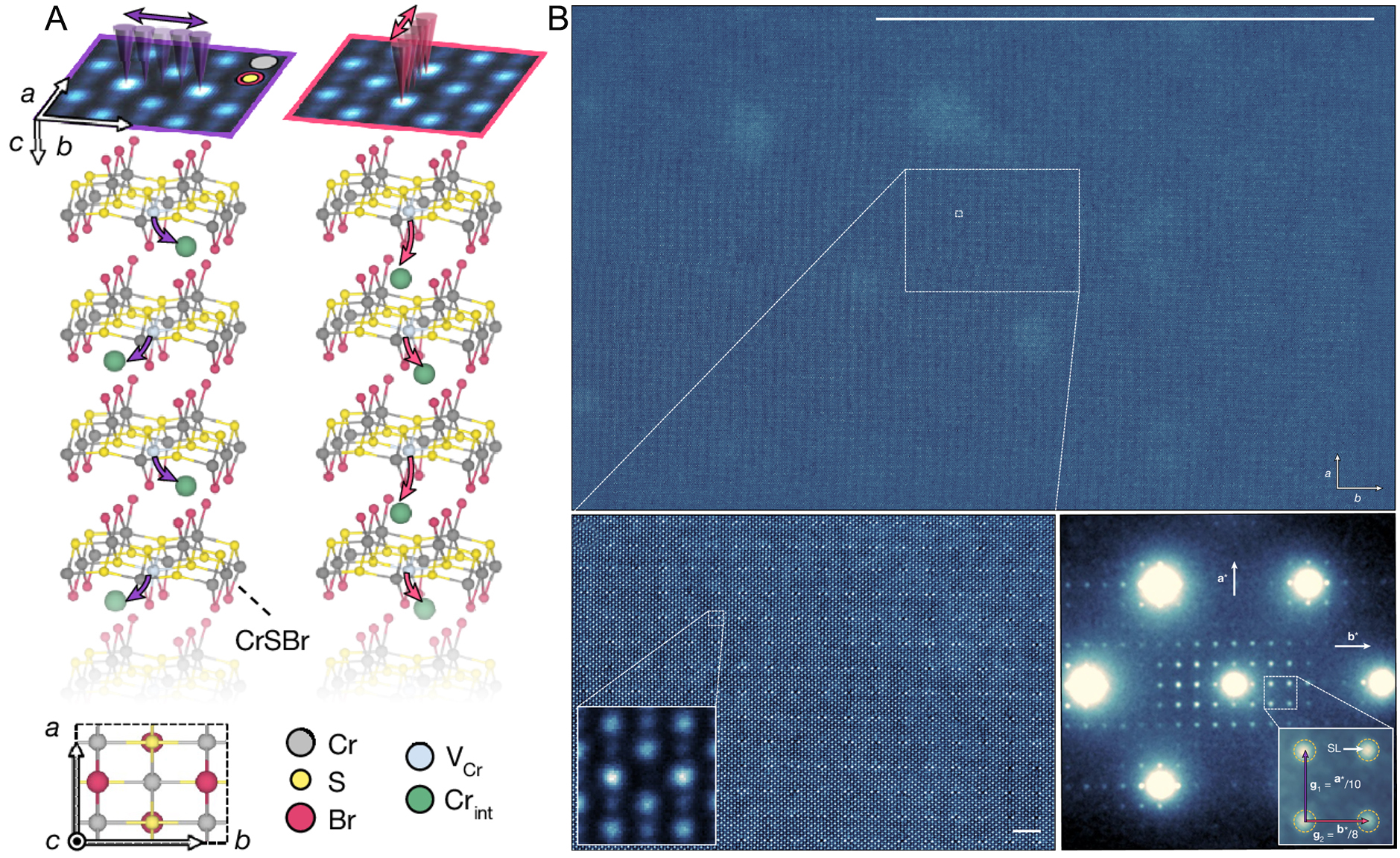
Figure 1. (A) Schematics and images showing the effect of a periodic beam motion on CrSBr crystal with a frequency of 0.5 kHz for 1 s in two directions. Cr atoms are displaced into the van der Waals gap, creating a Cr interstitial and a Cr vacancy at each layer of the crystal; (B) Three-dimensional mesoscopic defect crystal consisting of 79 × 58 locations in a volume of 150 nm × 100 nm × 13 nm. Diffraction pattern on the bottom right shows sharp superlattice Bragg reflections (inset) revealing the periodically modulated crystal-scale superstructure, indicating mesoscale order. Scale bars in the lower and higher magnification images are 0.1 μm and 2 nm, respectively. This figure reproduced from[1], Copyright 2026 Springer Nature.
A key advance of this work lies in demonstrating a paradigm shift of atomic manipulation from a local stochastic process into a deterministic programmable fabrication strategy. In this particular case, achieving reproducible defect formation at designated atomic positions required sub-20-picometer precision in electron beam positioning, and even slight beam offsets could lead to structural variations. By combining precisely designed beam trajectories with automated targeting workflows, the authors directed the beam between programmed target sites to create ordered arrangements of 4,582 defect columns, comprising over 40,000 user-defined defects across a 150 nm × 100 nm × 13 nm volume, in approximately 40 min
While this achievement establishes the viability of 3D mesoscale atomic engineering and represents a major step forward, translating deterministic fabrication into practical atomic manufacturing will require extending this capability across broader materials systems and establishing predictive control over fabrication outcomes. This requires identifying material-specific physical principles that govern energy transfer, atomic migration, defect formation, and structural stabilization under electron irradiation, and developing tailored strategies for different bonding environments, whether van der Waals, covalent, or ionic. Bridging this understanding to practice further demands quantitative beam-matter interaction models and inverse design frameworks that systematically connect electron beam parameters, such as incident energy, dose rate, and spatiotemporal trajectory, to targeted atomic configurations and functionalities. Data-driven approaches and deep learning may further accelerate this transition by navigating the complexity of high-dimensional fabrication parameter spaces and identifying fabrication strategies that remain transferable across materials systems[21].
Equally important, the next frontier of atomic manufacturing lies in extending structure modification/creation toward designed functionality realization. Integrating predictable fabrication with simultaneous characterization of emergent properties via techniques such as four-dimensional (4D)-STEM, electron energy loss spectroscopy, in-situ electrical transport or optical measurements, could enable dynamical mapping of local structure, chemistry, electronic states, optical responses and transport behavior during manipulation. A central challenge in this integration is the intrinsic write-read conflict: the same electron beam used for atomic manipulation also serves as the imaging and characterization probe, risking unintended modification of the as-modified structure. Nevertheless, advances in direct electron detection and deep-learning-enabled low-dose measurements are rapidly lowering the dose threshold for atomic-resolution readout[22,23], suggesting that the integration of fabrication and characterization into a unified workflow is becoming increasingly feasible. Establishing such closed-loop fabrication-characterization workflows would allow direct optimization of structure-property relationships and ultimately transform electron microscopy from a fabrication/imaging tool into a platform for creating and validating functional matter.
Realizing truly scalable atomic manufacturing will likely require a closed-loop framework that integrates prediction, fabrication, characterization and feedback optimization [Figure 2]. Artificial intelligence enabled control algorithms can automate electron-beam targeting and structural manipulation to improve reproducibility and to minimize unintended structural damage[24]. On-the-fly real-time detection and analysis further allow the microscopes to verify atomic configurations, dynamically adjust beam parameters, and steer specific structural rearrangements toward desired outcomes without continuous human intervention[25,26].
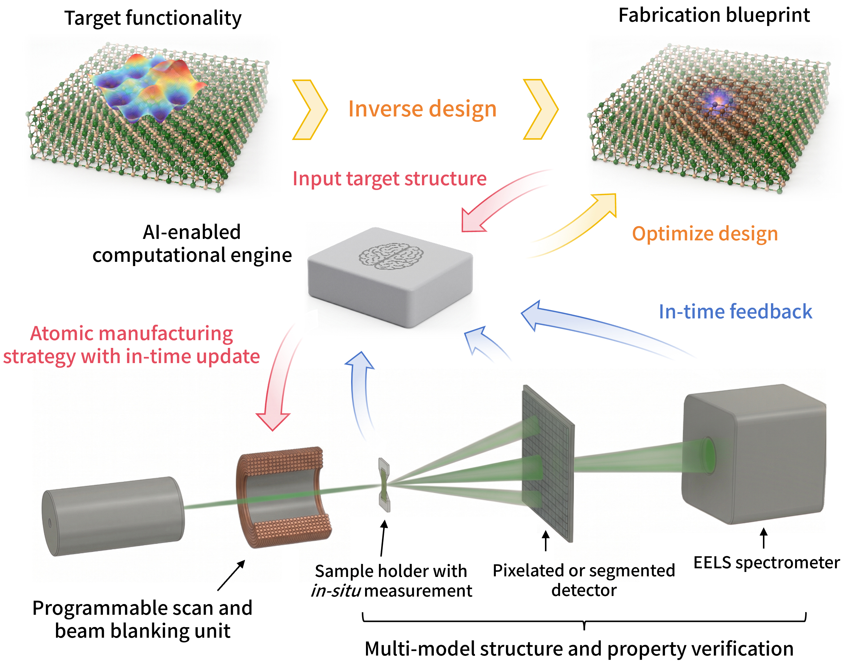
Figure 2. Conceptual illustration of closed-loop functional atomic engineering based on STEM.
Implementing this vision requires orchestration of beam positioning and dose allocation strategies that balance the disparate requirements of fabrication and different characterization modalities. Temporal synchronization of beam blanking, scan coils, and multimodal detectors must accommodate trade-offs among dwell time, signal-to-noise ratio, and acquisition speed, while spatial registration and drift correction need to maintain the positioning precision required for manipulation. Furthermore, feedback latency and real-time data throughput must be managed to ensure that in-situ measurements can inform subsequent beam-parameter adjustments without introducing unintended beam-induced damage. Importantly, integrating the aforementioned predictive beam-matter interaction models into the architecture enables an inverse design workflow: given a target atomic structure or functionality, the system could determine optimal fabrication parameters and initial manipulation strategies, while multimodal in-situ measurements continuously update these decisions during fabrication. Establishing such a closed-loop design-fabrication-characterization-feedback cycle may ultimately enable predictive, deterministic, and scalable functional atomic manufacturing.
The transition from deterministic atomic engineering to scalable atomic manufacturing could ultimately unlock transformative opportunities across multiple technological domains. Precisely arranging interacting, multi-orbital defect arrays may establish programmable platforms for solid-state quantum simulation and correlated quantum matter[1]. Controlled modulation of local crystal structures and phases could further enable direct electron-beam patterning of in-plane heterostructures, functional circuitry, and architected interfaces beyond the resolution limit of conventional nanofabrication. More broadly, tailoring structural symmetry and local interactions at the atomic scale may open new routes toward programmable metamaterials and devices with emergent functionalities[27].
Looking forward, advances in machine learning, integrated instrumentation, and autonomous experimentation[28] will further expand the scale, throughput, and complexity of electron-beam fabrication. The ultimate impact of atomic manufacturing will be determined not only by how precisely atoms are positioned, but also by how effectively their functionalities can be predicted, created, measured, and optimized. By integrating fabrication with multimodal characterization and closed-loop feedback, electron microscopy may ultimately transform from a structural characterization platform into a programmable atomic foundry capable of creating, measuring and optimizing functional matter across atomic, nano- and mesoscale dimensions.
DECLARATIONS
Authors’ contributions
Manuscript writing: Huang, S.
Manuscript review and editing: Zhou, W.; Huang, S.
Availability of data and materials
Not applicable.
AI and AI-assisted tools statement
During the preparation of this work, the authors used the AI tool Gemini 3.1 Flash Image (released 2026.05) solely for the rendering and optimization of the schematics in the Graphical Abstract and Figure 2. The tool did not influence the study design, data collection, analysis, interpretation, or the scientific content of the work. All authors take full responsibility for the accuracy, integrity, and final content of the manuscript.
Financial support and sponsorship
This work was supported by the China Postdoctoral Science Foundation (No. 2026M793763).
Conflicts of interest
Both authors declared that there are no conflicts of interest.
Ethical approval and consent to participate
Not applicable.
Consent for publication
Not applicable.
Copyright
©The Author(s)2026.
REFERENCES
1. Klein, J.; Roccapriore, K. M.; Weile, M.; et al. Mesoscale atomic engineering in a crystal lattice. Nature 2026, 653, 715-22.
2. Wang, H.; Fan, P.; Chen, J.; et al. Construction of topological quantum magnets from atomic spins on surfaces. Nat. Nanotechnol. 2024, 19, 1782-8.
3. Sierda, E.; Huang, X.; Badrtdinov, D. I.; et al. Quantum simulator to emulate lower-dimensional molecular structure. Science 2023, 380, 1048-52.
4. Bluvstein, D.; Evered, S. J.; Geim, A. A.; et al. Logical quantum processor based on reconfigurable atom arrays. Nature 2023, 626, 58-65.
5. Esat, T.; Borodin, D.; Oh, J.; et al. A quantum sensor for atomic-scale electric and magnetic fields. Nat. Nanotechnol. 2024, 19, 1466-71.
6. Kalff, F. E.; Rebergen, M. P.; Fahrenfort, E.; et al. A kilobyte rewritable atomic memory. Nat. Nanotechnol. 2016, 11, 926-9.
7. González-Herrero, H.; Gómez-Rodríguez, J. M.; Mallet, P.; et al. Atomic-scale control of graphene magnetism by using hydrogen atoms. Science 2016, 352, 437-41.
8. Klein, J.; Lorke, M.; Florian, M.; et al. Site-selectively generated photon emitters in monolayer MoS2 via local helium ion irradiation. Nat. Commun. 2019, 10, 2755.
9. Dyck, O.; Ziatdinov, M.; Lingerfelt, D. B.; et al. Atom-by-atom fabrication with electron beams. Nat. Rev. Mater. 2019, 4, 497-507.
10. Susi, T.; Kotakoski, J.; Kepaptsoglou, D.; et al. Silicon-Carbon bond inversions driven by 60-keV electrons in graphene. Phys. Rev. Lett. 2014, 113, 115501.
12. Lin, J.; Cretu, O.; Zhou, W.; et al. Flexible metallic nanowires with self-adaptive contacts to semiconducting transition-metal dichalcogenide monolayers. Nat. Nanotechnol. 2014, 9, 436-42.
13. Lin, Y.; Dumcenco, D. O.; Huang, Y.; Suenaga, K. Atomic mechanism of the semiconducting-to-metallic phase transition in single-layered MoS2. Nat. Nanotechnol. 2014, 9, 391-6.
14. Yang, S.; Sun, W.; Zhang, Y.; et al. Direct cation exchange in monolayer MoS2 via recombination-enhanced migration. Phys. Rev. Lett. 2019, 122, 106101.
15. Da, Y.; Luo, R.; Lei, B.; Ji, W.; Zhou, W. Controlled fabrication of freestanding monolayer SiC by electron irradiation. Chinese. Phys. B. 2024, 33, 086802.
16. Yin, K.; Zhang, Y.; Zhou, Y.; et al. Unsupported single-atom-thick copper oxide monolayers. 2D. Mater. 2016, 4, 011001.
17. Hudak, B. M.; Song, J.; Sims, H.; et al. Directed atom-by-atom assembly of dopants in silicon. ACS. Nano. 2018, 12, 5873-9.
18. Jesse, S.; Hudak, B. M.; Zarkadoula, E.; et al. Direct atomic fabrication and dopant positioning in Si using electron beams with active real-time image-based feedback. Nanotechnology 2018, 29, 255303.
19. Chen, C.; Wang, Z.; Lichtenberg, F.; Ikuhara, Y.; Bednorz, J. G. Patterning oxide nanopillars at the atomic scale by phase transformation. Nano. Lett. 2015, 15, 6469-74.
20. Jesse, S.; He, Q.; Lupini, A. R.; et al. Atomic-level sculpting of crystalline oxides: toward bulk nanofabrication with single atomic plane precision. Small 2015, 11, 5895-900.
21. Chen, I.; Aapro, M.; Kipnis, A.; Ilin, A.; Liljeroth, P.; Foster, A. S. Precise atom manipulation through deep reinforcement learning. Nat. Commun. 2022, 13, 7499.
22. Maclaren, I.; Macgregor, T. A.; Allen, C. S.; Kirkland, A. I. Detectors—The ongoing revolution in scanning transmission electron microscopy and why this important to material characterization. APL. Mater. 2020, 8, 110901.
23. Pate, C. M.; Hart, J. L.; Taheri, M. L. RapidEELS: machine learning for denoising and classification in rapid acquisition electron energy loss spectroscopy. Sci. Rep. 2021, 11, 19515.
24. Roccapriore, K. M.; Ross, F. M.; Klein, J. Quantitative electron beam-single atom interactions enabled by sub-20-pm precision targeting. Adv. Sci. 2025, 12, e02551.
25. Roccapriore, K. M.; Torsi, R.; Robinson, J.; Kalinin, S.; Ziatdinov, M. Dynamic STEM-EELS of atom and defect evolution during electron beam transformations. Microsc. Microanal. 2024, 30, ozae044.1007.
26. Boebinger, M. G.; Yilmaz, D. E.; Ghosh, A.; et al. Direct fabrication of atomically defined pores in MXenes using feedback-driven STEM. Small. Methods. 2024, 8, 2400203.
27. Yan, Z.; Handoko, A. D.; Wu, W.; et al. Atomic-engineered gradient tunable solid-state metamaterials. Proc. Natl. Acad. Sci. USA. 2024, 121, e2408974121.
Cite This Article
 Open Access
How to Cite
Huang, S.; Zhou, W. Towards deterministic and functional atomic manufacturing with electron beams. Microstructures 2026, 6, 20260121. https://dx.doi.org/10.20517/microstructures.2026.153
Download Citation
If you have the appropriate software installed, you can download article citation data to the citation manager of your choice. Simply select your manager software from the list below and click on download.
Export Citation File
Type of Import
Tips on Downloading Citation
Citation Manager File Format
Type of Import
Direct Import: When the Direct Import option is selected (the default state), a dialogue box will give you the option to Save or Open the downloaded citation data. Choosing Open will either launch your citation manager or give you a choice of applications with which to use the metadata. The Save option saves the file locally for later use.
Indirect Import: When the Indirect Import option is selected, the metadata is displayed and may be copied and pasted as needed.
About This Article
Copyright

Data & Comments
Data
0











Comments
Comments must be written in English. Spam, offensive content, impersonation, and private information will not be permitted. If any comment is reported and identified as inappropriate content by OAE staff, the comment will be removed without notice. If you have any queries or need any help, please contact us at support@oaepublish.com.