fig2

Zn doping modulation of carrier transport properties at the back interface of antimony sulfide solar cells

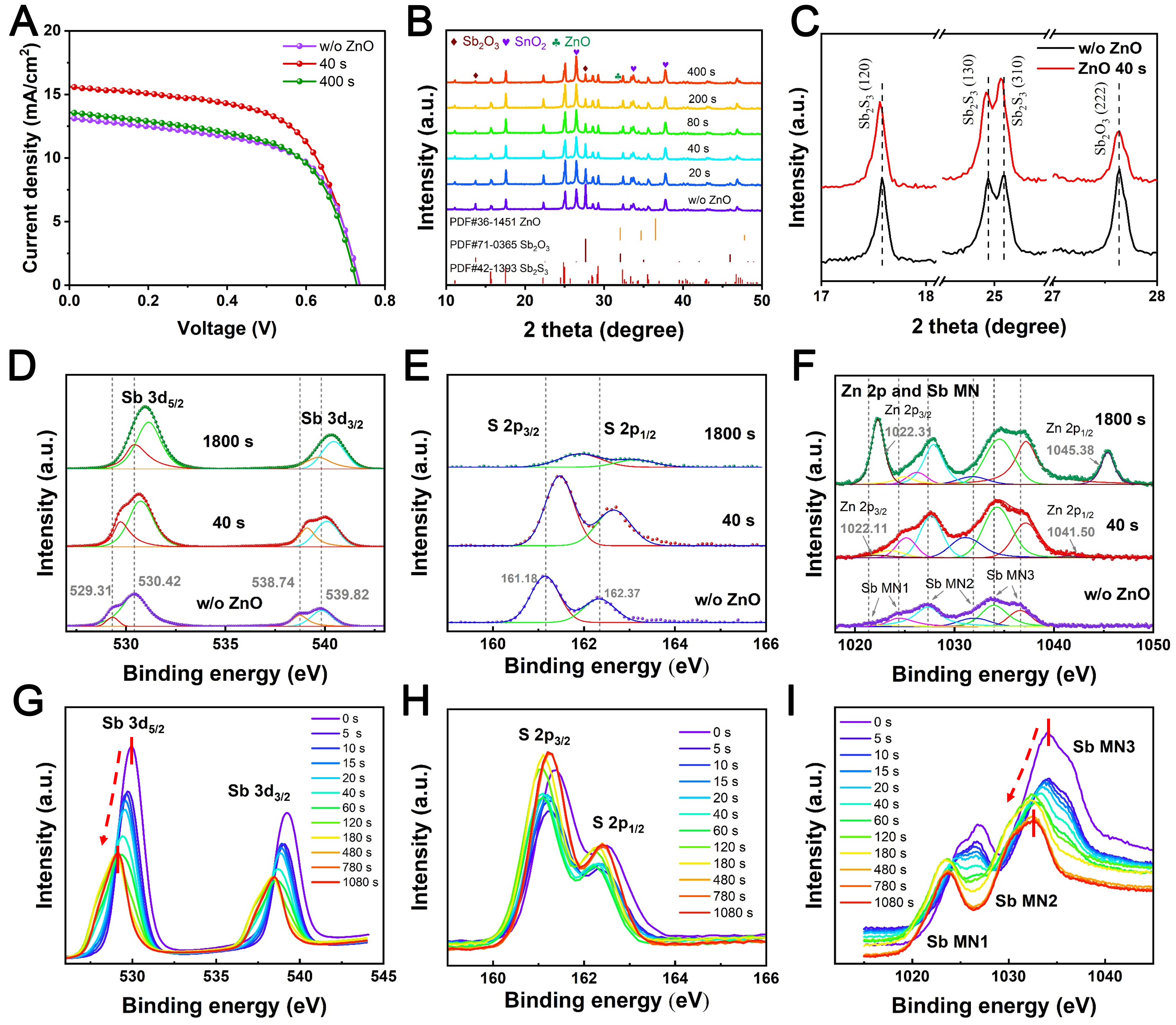
Figure 2. (A) J-V curves and (B) XRD patterns of Sb2S3 doped with ZnO with different deposition times; (C) The magnified XRD pattern of the Sb2S3 films; (D) Sb 3d, (E) S 2p and (F) Zn 2p XPS spectra of Sb2S3 thin films with and without ZnO. High-resolution (G) Sb 3d, (H) S 2p, (I) Sb MN XPS spectra. J-V: Density-voltage; XRD: X-ray diffraction; XPS: X-ray photoelectron spectroscopy; PDF: powder diffraction file; MN: X-ray photoelectron spectrum peak of Sb; W/O: without ZnO.

Energy Materials
ISSN 2770-5900 (Online)
Follow Us

Portico

All published articles are preserved here permanently:

https://www.portico.org/publishers/oae/

Portico

All published articles are preserved here permanently:

https://www.portico.org/publishers/oae/