fig1

 <i>In-situ</i> construction of artificial interface layer using sodiophilic Bi<sub>2</sub>S<sub>3</sub> nanowires for dendritic-free sodium-metal batteries

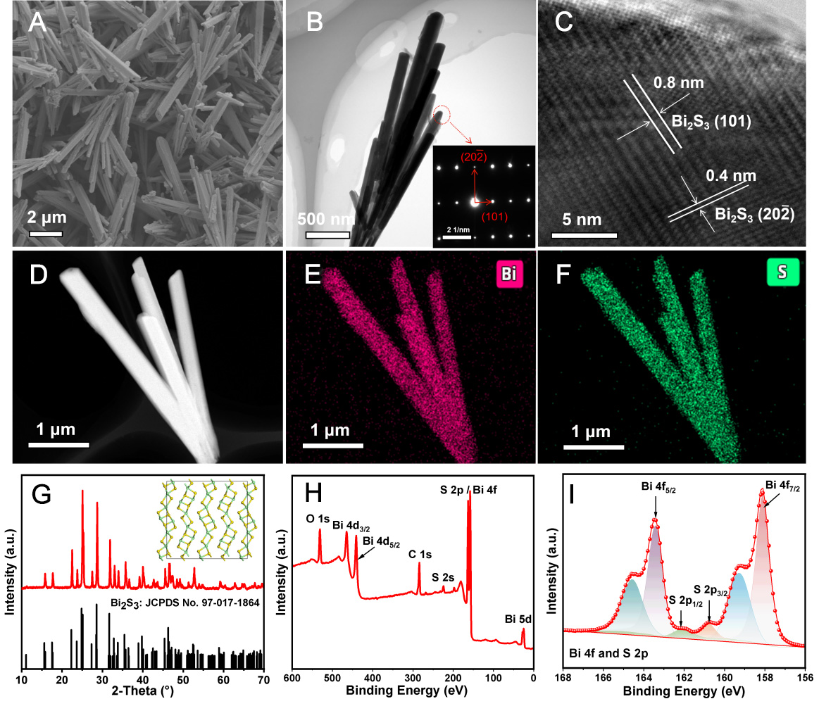
Figure 1. (A) SEM image, (B) TEM image with SAED pattern, and (C) HRTEM image of Bi2S3 nanowires; (D) HAADF-STEM image and (E and F) corresponding EDS maps of (E) Bi and (F) S elements for a bundle of Bi2S3 nanowires; (G) XRD pattern with inset showing the supercell structure of Bi2S (Yellow balls stand for Bi atomic sites, and green balls for S atoms); (H) Survey XPS spectrum, and (I) Bi 4f/S 2p XPS spectra of Bi2S3 nanowires. SEM: Scanning electron microscope; TEM: transmission electron microscope; XPS: X-ray photoelectron spectroscopy; XRD: X-ray diffraction; HRTEM: high-resolution transmission electron microscopy; HAADF-STEM: high-resolution transmission electron microscopy; SAED: selected area electron diffraction.

Energy Materials
ISSN 2770-5900 (Online)
Follow Us

Portico

All published articles are preserved here permanently:

https://www.portico.org/publishers/oae/

Portico

All published articles are preserved here permanently:

https://www.portico.org/publishers/oae/