fig1
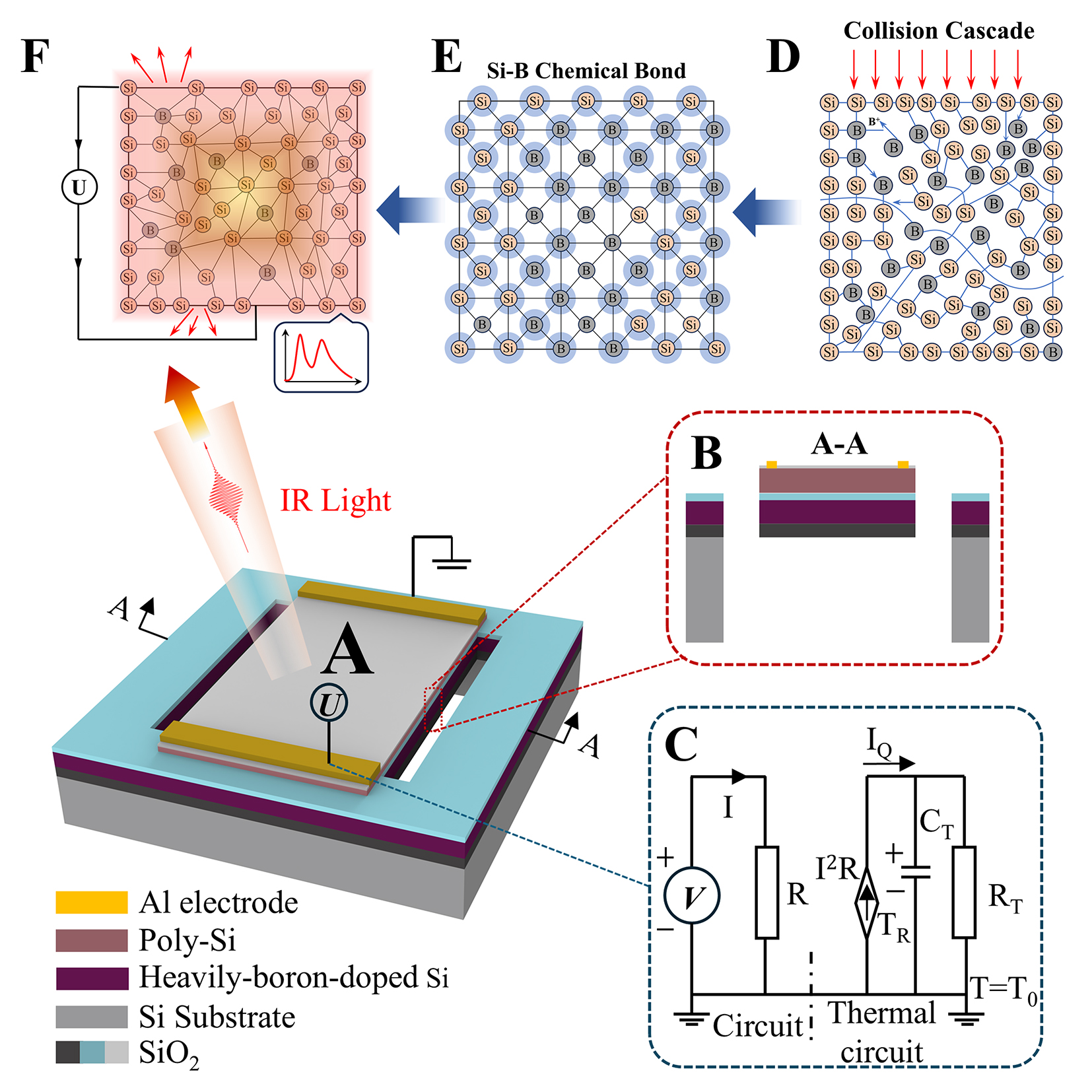
Figure 1. Schematic of the proposed MEMS infrared-light-source chip. (A) 3D model; (B) Cross-sectional view along the A-A plane; (C) Equivalent circuit diagram illustrating the working principle of the MEMS-based suspended membrane infrared-light-source chip; (D) Atomic distribution map of boron ion implantation; (E) Schematic of Si-B bond formation after annealing; (F) Atomic-level schematic of electrothermal radiation in B-doped polycrystalline silicon.