


Degradation by design: sequentially degradable organic transistors for sustainable electronics
 0
0 Abstract
The growing accumulation of electronic waste (e-waste) and demand for environmentally sustainable technologies have accelerated interest in transient degradable electronics, which physically disintegrate or biodegrade after their functional lifetime. Such devices offer promising pathways towards reducing ecological impact while enabling applications in biomedical implants, environmental sensors, and temporary wearable systems. Biodegradable organic thin-film transistors (OTFTs) play a pivotal role as fundamental building blocks for fully transient electronic circuits, combining mechanical flexibility, solution processability, and controlled disintegration. In this study, we report the development of a fully degradable OTFT fabricated using diketopyrrolopyrrole thiophene-imine-thiophene as the biodegradable semiconducting layer, integrated with a bilayer dielectric composed of poly(vinyl alcohol) (PVA) and poly(caprolactone) (PCL), and a poly(lactic acid) (PLA) substrate. This configuration yields a significant reduction in threshold voltage (VT) from -16.1 to -2 V compared to devices fabricated on octyltrichlorosilane/SiO2, while maintaining comparable charge carrier mobility. The OTFT can be selectively degraded through sequential steps, where the semiconductor dissolves under acidic conditions (1 M HCl), followed by degradation of the dielectric and substrate in basic buffer solution. This controlled disassembly enables separation and potential recycling of individual components, providing a straightforward strategy for environmentally responsible end-of-life management of transient electronics. Overall, this work represents an important step toward realizing low-voltage, fully degradable, and recyclable electronic systems for sustainable applications.
Keywords
INTRODUCTION
The rapid growth of electronic devices across biomedical, environmental, and consumer applications has intensified concerns over electronic waste (e-waste) and the long-term persistence of electronic materials. Transient electronics address this challenge by incorporating materials that undergo controlled degradation after use, thereby reducing waste accumulation and environmental impact[1-3]. These biodegradable electronics have several advantages, such as (i) lowering the amount of e-waste that accumulates; (ii) circumventing invasive surgeries to remove implanted devices; and (iii) enabling environmental transience, which allows sensors that are deployed remotely to function without retrieval[4-7]. Organic thin-film transistors (OTFTs) are electronic building blocks for circuits with applications in biological and chemical sensors[8], health monitoring systems[9], stretchable electronics[10], and electronic skin[11]. While advances in materials design have greatly improved OTFT performance, the environmental and biological safety of these materials remain underexplored[12,13].
Advancing transient OTFT requires deliberate design and scalable fabrication of each component and layer to ensure both performance and sustainability[14-17]. Lei et al. demonstrated the fabrication of a biocompatible and fully disintegrable OTFT, with respectable charge carrier mobility, using a semiconducting polymer with iron electrodes and a cellulose substrate[18]. They reported complete disintegration of their OTFTs in acidic conditions after 30 days in-vitro. However, when all components degrade simultaneously in a single environment, it becomes difficult to separate, isolate, or recycle functional materials. Thus, advancing fully transient electronics requires OTFTs in which each component responds to distinct degradation triggers, enabling controlled disassembly and targeted recovery of valuable resources like gold/precious metals.
The substrate, which accounts for 99.89% of the overall device mass[19], must be a biodegradable plastic. Biobased materials such as poly(lactic acid) (PLA), polyhydroxyalkanoates (PHAs), starch blends, and cellulose-derived polymers are promising substrate options, contingent upon processing temperatures not exceeding ~150 °C[20]. However, biodegradable dielectrics exhibiting appropriate physical and electrical properties remain limited. Poly(vinyl alcohol) (PVA) [Figure 1] is a bioresorbable dielectric that rapidly dissolves in environmentally benign solvents such as water and undergoes natural degradation when exposed to suitable bacteria[21]. PVA has been utilized as a dielectric in sensors and OTFTs, either in its pure polymer form or in combination with other materials[22-24]. Despite its benefits, PVA presents challenges: printing frequently necessitates optimization, such as the incorporation of viscosity enhancers, and its hydrophilic characteristics render the resultant films susceptible to moisture, undermining device stability and reliability[25,26]. Previously, our group demonstrated that combining PVA with an interfacial, thermally crosslinked diisocyanate-terminated poly(caprolactone) (TPCL) yields a high-performance, hydrophobic, and degradable high-k/low-k bilayer dielectric[27,28]. This architecture couples the high dielectric constant and electrical performance of PVA with the moisture resistance of poly(caprolactone) (PCL), while also improving surface compatibility for semiconductor deposition[29,30]. To enhance shelf stability and enable scalable processing, we further synthesized benzodioxinone-terminated PCL, which can be ultraviolet (UV)-coupled to the PVA surface [Figure 1][24,26]. PLA, PVA, and PCL are inexpensive, widely available, and have a long history of use in biomedical devices within clinical practice[19].
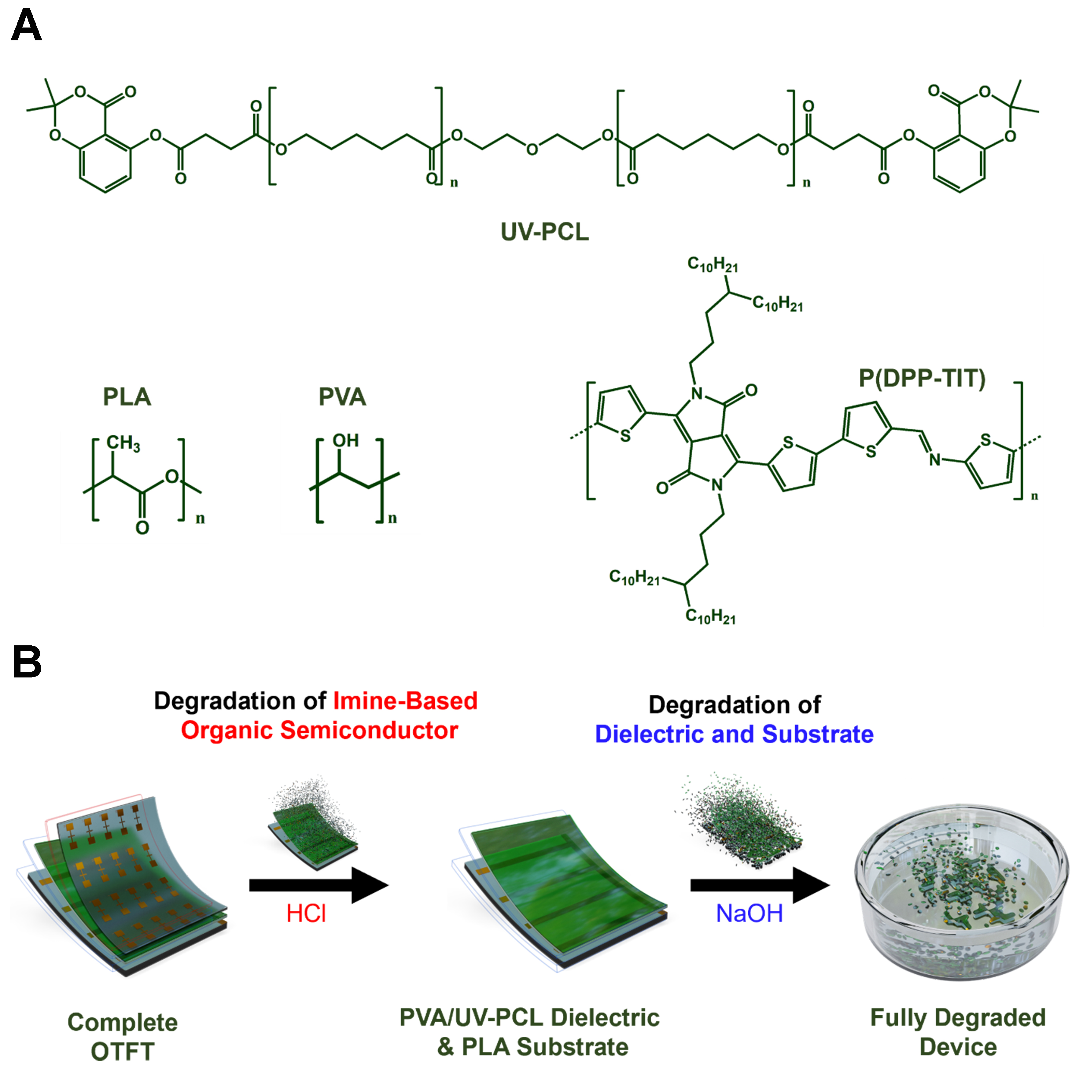
Figure 1. (A) Chemical structures of biodegradable polymers: PLA, PVA, benzodioxinone-terminated poly caprolactone (UV-PCL), and P(DPP-TIT); (B) Schematic illustration of the sequential degradation of an OTFT device. All elements in this figure were developed using ChemDraw and Blender. PLA: Poly(lactic acid); PVA: poly(vinyl alcohol); UV: ultraviolet; PCL: poly(caprolactone); P(DPP-TIT): poly diketopyrrolopyrrole-thiophene-imine-thiophene; OTFT: organic thin-film transistor.
A diverse array of processing and synthetic strategies have been developed and optimized towards designing transient organic semiconductors, primarily focused integrating and balancing electronic functionality with environmental instability[31]. These approaches include encapsulation of semiconducting fillers within biodegradable polymer matrices, the synthesis of block copolymers featuring discrete semiconducting and degradable segments, the utilization of naturally occurring pigments susceptible to enzymatic breakdown, and the covalent tethering of conjugated motifs to degradable scaffolds via chemically cleavable linkages[32-34]. Among these strategies, the integration of acid-labile imine motifs directly within the backbone of organic conjugated polymers is a promising approach for designing materials possessing good electronic performance while also foregoing the requirement of complicated degradation triggers[18,35]. Compared to other strategies which rely on either disrupting the conjugated backbone or reducing the amount of semiconducting material within the device’s active layer, imine-motifs possess sp2-hybridization character, allowing for the double-bond to contribute and maintain the orbital delocalization of the conjugated polymer backbone, a parameter critical for obtaining good charge carrier mobility in OTFTs[36-38]. Furthermore, compared to other synthetic approaches for designing transient organic semiconductors, imine-based conjugated polymers do not require complicated synthetic protocols or specialized processing procedures, and have shown potential promise for greener synthetic pathways in developing organic semiconductors[39,40]. When paired with an established high charge carrier performance chemical structure, particularly diketopyrrolopyrrole (DPP), it has been demonstrated that imine-based conjugated polymers can be used to fabricate high performance transient OTFTs with measurable electronic properties comparable to conventionally used designs[37]. In addition to possessing good charge carrier mobility in OTFTs, DPP-based polymers have well-understood aqueous and photo-degradation mechanisms, further enforcing their role as promising chemical motifs for designing transient devices that are also environmentally benign[41,42]. Inspired by previous reports, DPP was copolymerized with a thiophene-imine-thiophene donor monomer to generate poly diketopyrrolopyrrole thiophene-imine-thiophene [P(DPP-TIT)], a conjugated polymer established to have good hole charge carrier mobility in OTFTs[36,43].
To further synergize good electronic performance with degradation capabilities, we report a novel variant of P(DPP-TIT), as per Figure 1, designed with alkyl side chains where each branching arm symmetrical carbon lengths, a structural feature known to enhance charge transport in thin films while simultaneously limiting excessive molecular weight growth during polymerization, allowing for relatively narrow dispersity in polycondensation-type reactions[44,45]. The combination of narrow dispersity and lower molecular weight of the organic semiconductor has implications in accelerating degradation time, a highly sought after trait in transient electronic technologies[46]. By integrating the P(DPP-TIT) conjugated polymer with degradable polymeric substrates and dielectric layers, it is possible to design fully transient OTFTs that exhibit strong electrical performance while producing benign by-products during degradation. The combination of materials with distinct degradation triggers enables controlled, multi-step disassembly that allows selective breakdown, separation, and potential recycling of individual layers. Finally, incorporating biocompatible, non-toxic electrodes alongside these materials completes the foundation for fully biodegradable and biocompatible electronic devices. We have previously fabricated cytocompatible and disintegrable OTFTs using gold electrodes; however, the gold electrodes did not degrade and therefore required recovery[24]. Gold combines high electrical conductivity and excellent biocompatibility in both in vitro and in vivo environments, and is well-established role in various medical technologies[47-49]. Furthermore, as an inert biomaterial, gold has proven effective in reducing biofouling in biological systems[50], particularly in implants such as cardiovascular devices and biomedical microelectromechanical systems (BioMEMS)[51].
This study presents a fully degradable and biocompatible p-type OTFT with high mobility and low threshold voltage (VT), based on a P(DPP-TIT) conjugated polymer integrated with a biodegradable PLA substrate and a bilayer PVA/UV-PCL dielectric. Low-temperature surface engineering strategies, including the deposition of biodegradable hydrophobic interlayers, were employed to improve film quality and device reproducibility. Electrical performance and stability were benchmarked against conventional OTFT architectures, confirming competitive operation while highlighting the advantages of sustainable materials. Distinct from previous reports, each device component in this system degrades under a specific pH trigger, enabling sequential disassembly and selective recovery of individual layers [Figure 1B]. The imine-containing P(DPP-TIT) semiconductor dissolves under acidic conditions, whereas the PLA substrate and dielectric degrade in basic environments, allowing controlled separation and recycling. This dual-trigger design establishes a new paradigm for transient optoelectronics, demonstrating how performance and sustainability can be co-engineered through programmable end-of-life disassembly.
EXPERIMENTAL
Materials
All reagents were acquired from Sigma-Aldrich and utilised without additional purification unless specified differently. Octyltrichlorosilane (OTS, 97%) was dissolved in anhydrous toluene (99.8%) inside a glovebox to prepare a 1% v/v solution. PCL diol (Mw = 2,000 Da), toluene-2,4-diisocyanate (95%), PLA (230 kg·mol-1), and PVA (Mw = 31,000-50,000 Da; 98%-99% hydrolyzed) were procured from Sigma-Aldrich. Chromium-coated tungsten rods and high-purity gold (Au, 99.99%) were obtained from Angstrom Engineering. Quartz-coated glass substrates (15 × 20 mm2) were acquired from Ossila Limited, whereas Si wafers featuring a 230 nm SiO2 layer and shadow masks were provided by WaferPro and Ossila Limited, respectively. Deuterated chloroform (99.8% purity) and benzene (98% purity) were obtained from Cambridge Isotope Laboratories Inc. The synthesis of P(DPP-TIT) was conducted according to established protocols, and 2,2-dimethyl benzodioxinone-terminated PCL (UV-PCL) was synthesised using documented methods[27].
Gel permeation chromatography
Number average molecular weight (Mn), weight average molecular weight (Mw), and polydispersity index (PDI) of P(DPP-TIT) were evaluated by high temperature size exclusion chromatography (SEC) [Supplementary Figure 1 and Supplementary Table 1] using 1,2,4-trichlorobenzene (TCB) and performed on S-3 an EcoSEC HLC-8321GPC/HT (Tosoh Bioscience, Japan) equipped with a single TSKgel GPC column (GMHHR-H; 300 mm × 7.8 mm) calibrated with monodisperse polystyrene standards. The samples were prepared using 1 mg/mL of sample in TCB, which were allowed to stir at 80 °C for 12 h prior to injection. The analysis of the samples was performed at 180 °C with a flow rate of 1.0 mL/min with injection quantities of 300 µL. The data was collected and integrated using EcoSEC 8321GPC HT software suite.
Preparation of the substrate and dielectric
The Substrate (PLA) and dielectric (PVA/UV-PCL) solutions were prepared following the protocol reported in our previous study[24]. Briefly, the materials were dissolved in the appropriate solvent systems under continuous stirring until complete homogenization was achieved. The processing conditions, including concentration, temperature, and mixing duration, were maintained consistent with the previously optimized procedure. Detailed processing parameters and preparation steps can be found in our earlier publication[24].
Fabrication of OTFTs
Glass substrates (15 × 20 mm2) coated with quartz were used as temporary supports for the fabrication of OTFTs. Substrate cleaning and preparation were carried out according to the protocol described in our previous study[52].
A spin coater [Laurell WS-650-23, United States of America (USA)] was used to spin-coat the PLA solution in chloroform (70 mg/mL) filtered through 0.22-micron polytetrafluoroethylene (PTFE) filters, onto the cleaned substrates for 90 s at 1,200 rpm. The substrates were then vacuum annealed for 15 min at 70 °C. PLA films with a thickness of roughly 2 μm were produced by this method. The gate electrodes were deposited using a thermal evaporator (Angstrom Evovac, Canada), consisting of a 2 nm chromium (Cr) adhesion layer (0.5 Å·s-1) and a 50 nm gold (Au) layer (0.5 Å·s-1) applied to the PLA film through a shadow mask. After that, the PLA substrates coated with Cr/Au were air-plasma-treated using PDC-32G plasma cleaner (Harrick Plasma, USA) for 15 min, followed by rinsing with isopropanol and water, which improved surface wettability. Next, the biodegradable bilayer dielectric layers were deposited following our previously reported procedure[24]. After crosslinking the degradable semiconducting layer was deposited by spin-coating a
Device characterization
OTFT were characterized using a Keithley 2614B source meter coupled to a specially designed auto-tester[53]. The complete device characterization procedure can be found in the Supplementary Materials.
Thin film characterization
Grazing-incidence wide-angle X-ray scattering
Grazing-incidence wide-angle X-ray scattering (GIWAXS) experiments were performed at the SOLEIL Synchrotron facility in Saint-Aubin, France, using the SIRIUS beamline[54]. The X-ray energy was set to
Atomic force microscopy
Atomic force microscopy (AFM) images were taken using an AFM (Bruker Dimension FastScan, USA) with ScanAsyst-Air tips in Peak Force Tapping Mode. Imaging processing was performed with NanoScope Analysis v.3.0. The samples per line used were 512.
Raman spectroscopy
A confocal Raman microscope [Renishaw inVia InSpec, United Kingdom (UK)] was used to record non-polarized Raman spectra, in conjunction with a Leica Microsystems DM2700 bright-field microscope, Germany. Spectra and maps for P(DPP-TIT) films on SiO2 and bilayer dielectrics were collected in the 500-2,000 cm-1 range using a 532 nm laser (500 mW) and a 2,400 L·mm-1 grating. The laser beam was focused onto the sample through a 50 L with a 0.5 aperture integrated into the DM2700 optical system. This setup provided a theoretical depth of focus of approximately 3.0 µm, a spatial resolution of about 640 nm, and a spectral resolution of 0.3 cm-1 [full width at half maximum (FWHM)]. Calibration was performed before each measurement using the silicon reference peak at 520 cm-1, maintained within ± 0.5 cm-1 accuracy. Raman spectra were collected without polarization at 10% laser power (50 mW) and a 10 s exposure time. Raman mapping (19 × 19 µm2) was performed using 361 individual spectra, acquired with a 1.0 µm step size, 5% laser power (25 mW), and a 10 s exposure. All data were processed to remove cosmic ray artifacts.
UV-visible spectroscopy
A Cary 6000i UV-Vis-NIR spectrophotometer (Agilent Technologies, Malaysia) was used to collect spectra. Absorbance measurements were collected for solid-state thin films deposited onto a glass substrate via drop casting, followed by annealing at 50 °C for 1 h, within the range of 250-1,000 nm.
Profilometer
A Dektak XT Profilometer (Bruker Corporation, USA) was used to measure the thickness of the PLA substrates, bilayer dielectrics, and P(DPP-TIT) films.
RESULTS AND DISCUSSION
Fully transient OTFTs were fabricated using biocompatible and biodegradable polymers chosen for their electrical performance, processability, and distinct degradation behavior. The devices feature a bottom-gate, top-contact (BGTC) architecture where Figure 1 shows the chemical structures of the PLA substrate, PVA/UV-PCL bilayer dielectric, and P(DPP-TIT) semiconductor, along with a schematic of the stepwise degradation. A uniform biodegradable PLA film was obtained by spin coating PLA onto a quartz-coated glass substrate which was baked to eliminate residual solvent, following established literature[56,57]. The resulting PLA substrate was approximately 2 μm thick and was subsequently coated with patterned chromium and gold (Cr/Au) electrodes. The chromium interlayer facilitated strong adhesion between the gold film and the PLA surface and functioned as the bottom gate electrode, ensuring stable and reproducible electrical characterization[53]. Since the gold-patterned PLA surface exhibited hydrophobic characteristics[24], air plasma treatment for 15 min was employed to enhance its surface hydrophilicity, thereby facilitating uniform coating of the subsequent dielectric layer. The PVA dielectric layer was deposited by spin-coating on the gold/PLA substrate and was annealed at low temperatures (50 °C for ~18 h). We found that exposure of the PLA substrate to temperatures > 50 °C results in dimensional shrinkage, leading to surface buckling and increased roughness, conditions unfavorable for OTFT fabrication[24]. Hygroscopic polymer dielectrics, such as PVA, can demonstrate a capacitance density enhancement of up to ×50 at 10 Hz upon moisture exposure[58]. This phenomenon occurs as water functions as a plasticizer, facilitating the alignment of hydroxyl groups in an electric field and thereby augmenting the capacitance of PVA films[59,60]. However, for flexible electronic circuits, it is essential to preserve constant dielectric characteristics and avoid water uptake. A thin PCL layer (about 1-2 nm) applied to the PVA layer provides efficient moisture barrier properties, hence leading to more reliable and predictable electronic performance[24,60,61]. Therefore, following the PVA annealing, we deposited a hydrophobic interlayer (UV-PCL) to improve film quality and device reproducibility. The optimal UV-crosslinking conditions were previously determined through solvent-resistance testing using toluene and by measuring the water contact angle before and after rinsing in our previous studies[24,27]. The interfacial cross-linking between PCL and PVA not only stabilizes the dielectric bilayer by anchoring the PCL film to the underlying PVA matrix[52,62] but also suppresses polymer aggregation and reduces the density of surface hydroxyl groups that can act as charge-trapping sites during OTFT operation[63]. The remaining hydroxyl functionalities within the bulk of the PVA contribute to a relatively high dielectric constant (k), while the cross-linked top layer enables orthogonal solution processing for subsequent semiconductor deposition[64,65]. The dielectric properties of the resulting bilayer dielectric (PVA/UV-PCL) were assessed by impedance spectroscopy, with the findings presented in Table 1. The reported dielectric constant values aligned with the anticipated range for PVA[22,24,58,66].
Dielectric properties of bilayer dielectric (PVA/UV-PCL) at 10 Hz
| Dielectric | Effective dielectric constant (k) | Capacitance density (nF/cm-2) |
| PVA/UV-PCL | 6.6 ± 3.2 | 19.7 ± 9.7 |
P(DPP-TIT) was deposited on the UV-PCL layer by the spin-coating followed by vacuum annealing for 1 h at 50 °C. For performance benchmarking, P(DPP-TIT)-based OTFTs were also fabricated using OTS-treated SiO2 as the gate dielectric, employing an identical device architecture to ensure direct comparison with the degradable OTFTs[22,58,60,66-68]. Finally, gold contacts were deposited on the semiconducting layer as the source/drain electrodes. Figure 2A-D display the characteristic output and transfer curves of both OTFTs. Performance parameters, including field-effect hole mobility (µh), VT, and on/off current ratio (Ion/off) were extracted to quantify electrical performance [Table 2]. The VT of P(DPP-TIT) OTFTs reduced markedly from -16.1 ± 0.9 V on OTS-treated SiO2 gate dielectrics to -2.0 ± 0.4 V with the application of a PVA/UV-PCL bilayer dielectric. The decrease in VT indicates less polarity at the semiconductor/dielectric interface, hence mitigating charge trapping[27,69-71]. This can be attributed to the enhanced dielectric constant of the PVA/UV-PCL bilayer (~6.6) in comparison to SiO2 (3.9) at frequencies under 1 kHz[72] as well as the elimination of hydroxy group-based charge traps due to the interfacial crosslinking with UV-PCL[24]. These values represent a significant improvement compared to previous studies[19] in which PVA was solely employed as a dielectric, yielding VT values of around -15.4 V for biocompatible and bioresorbable OTFTs. The highest µh of the functional OTFT was statistically similar, measuring 0.17 cm2·V-1·s-1 for OTFT made with OTS-treated SiO2 dielectric and 0.16 cm2·V-1·s-1 for OTFT fabricated with PVA/UV-PCL dielectric. The Ion/off for PVA/UV-PCL based devices is low and typical for PVA-based dielectrics[73]; resulting from the low VGS and VSD needed to operate the device. For example, when the OTFT fabricated with PVA/UV-PCL bilayer dielectric was tested at VGS and VSD = -5 V, we obtained approximately 0.85 μA, but the OTFT made using OTS/SiO2 dielectric remained inactive under the same conditions, requiring approximately -10 V to obtain the same amount of current. While mild hysteresis is observed in the PVA/UV-PCL OTFTs due to the dielectric environment and interfacial characteristics, these results demonstrate an effective strategy for developing fully biodegradable, high-performing devices. The on-current value was extracted from the output characteristics at VGS = -5 V and VDS = -5 V. A lower current level (~0.2 μA) is observed in the transfer characteristics measured under the same bias conditions, which can be attributed to transient charge trapping and bias-stress effects commonly observed in polymer dielectric-based field-effect transistors.
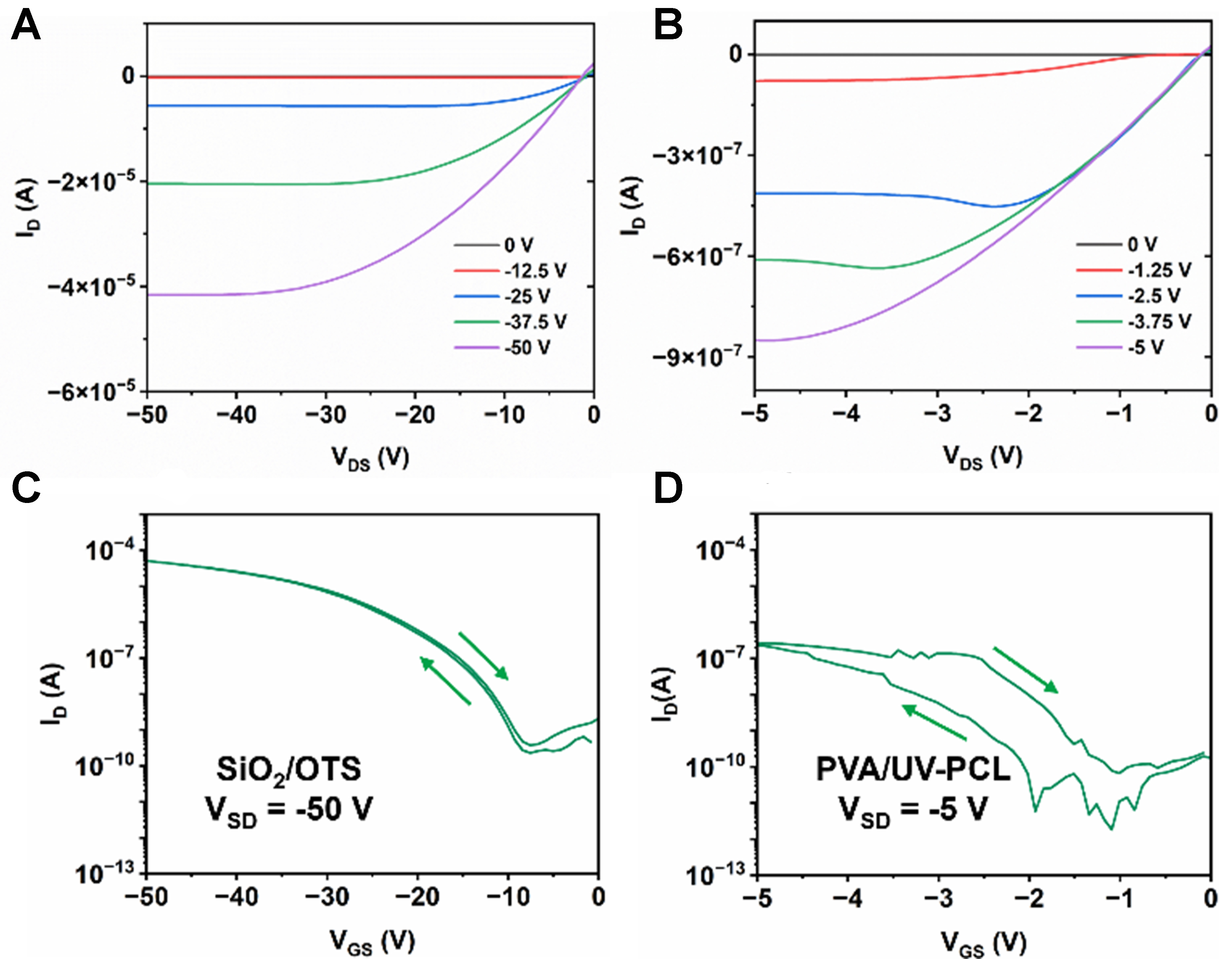
Figure 2. Output curves of (A) SiO2/OTS and (B) PVA/UV-PCL, and characteristic transfer curves of (C) OTFTs on OTS-treated SiO2 and (D) on PVA/UV-PCL. The transfer curves vs. VGS were acquired at VDS = -50 V and VDS = -5 V, respectively. Transfer curves and leakage current are plotted under identical bias conditions for four times for a representative device in the Supplementary Figure 3. OTS: Octyltrichlorosilane; PVA: poly(vinyl alcohol); UV: ultraviolet; PCL: poly(caprolactone); OTFTs: organic thin-film transistors.
Summary of the field effect properties of the degradable and non-degradable OTFT
| Substrate/gate/dielectrica | Mobility (cm2·V-1·s-1) | Ion/off d | VT (V)c | ne | |
| µmax b | µavg c | ||||
| Si/SiO2 | 0.17 | 0.08 ± 0.04 | 104 | -16.1 ± 0.9 | 38 |
| PLA/Au/PVA/UV-PCL | 0.16 | 0.03 ± 0.04 | 103 | -2.0 ± 0.4 | 31 |
In our study, we observe the expected tradeoff between fully green, transiently degradable dielectrics and OTFT performance. Hysteresis mainly originates from slow polarization and charge trapping associated with the polar hydroxyl groups in the PVA dielectric[24,27]. PVA contains a high density of hydroxyl groups, whose dipoles reorient under the applied gate field but relax on a timescale comparable to, or slower than, the voltage sweep, this time-dependent dipolar polarization makes the channel charge depend on the sweep direction, giving rise to a hysteretic shift and current. Moisture uptake can further facilitate reorientation of hydroxyl groups or introduce additional mobile charges, modifying but not eliminating this hysteresis, while added low-k interlayers (e.g., UV-PCL) mainly lower interfacial charge trapping and leakage but do not completely remove the intrinsic dipolar polarization effects[24,27,28,61]. In a previous study from our group[27], we showed that hysteresis can be largely suppressed by lowering pulsing frequency, confirming that the dominant contribution is dielectric polarization. In addition, these devices were measured over a much lower voltage range (VGS and VSD = -5 V) compared to SiO2-based devices VGS and VSD = -50 V) to achieve their low-voltage operation, which explains the smaller drain current values. Nevertheless, despite these trade-offs, the devices still exhibit clear transistor behavior with reproducible channel formation at low voltages, demonstrating that the PVA/UV-PCL dielectric system enables functional, low-voltage, transient electronics as intended.
Furthermore, to evaluate short-term bias stability, consecutive transfer characteristics were measured under identical bias conditions. Supplementary Figure 2A-D, depicts the representative transfer curves. The device exhibited minimal variation in extracted parameters over four repeated sweeps [Supplementary Table 2], indicating stable charge transport and limited bias-induced degradation within the measurement time scale.
We performed numerical simulation to investigate the mechanism of the fabricated P(DPP-TIT) TFTs[74-78]. Our goal was to reconstruct the transfer characteristics measured under dual-sweep conditions for the devices representative for the non-degradable (SiO2 dielectric) and degradable (PVA/UV-PCL dielectric) systems. We found that all curve groups measured in the saturation regime reasonably well follow the quadratic ID-VG relationship, excluding the Schottky barrier and/or trap effects as a dominant contributor. We therefore took the hole mobility μsim (intrinsic mobility that serves as a simulation input) and the charge density at the semiconductor/insulator interface Nint as main fitting parameters.
Supplementary Figure 4A and B show the results of optimized simulation fitting to the experimental data. The fitting process yielded μsim of 0.112 and 0.051 cm2·V-1·s-1 for the non-degradable and degradable devices, respectively. The dual-sweep measurement, conducted in the sequence of off-to-on and on-to-off scans, resulted in a hysteresis in opposite directions to a different extent in the two TFTs. The dynamic shift of the VT due to the hysteresis was modelled by the modulation of Nint in our simulation. As shown in Supplementary Figure 4C, the degradable TFT showed significantly lower Nint values as compared to the non-degradable TFT, confirming the suitability of the P(DPP-TIT) semiconductor–PVA/UV-PCL dielectric combination for low-voltage applications. The small hysteresis of the non-degradable TFT [Figure 2C] was tracked by a slight increase in Nint between the two scans. The larger and opposite-direction hysteresis of the degradable TFT [Figure 2D] was modelled by a decrease in Nint, which could originate from slower relaxation associated with charged species in the multi-component PVA/UV-PCL dielectric. Nint is the fixed two-dimensional charge density at the semiconductor/insulator interface that either partially screens or reinforces the externally applied gate field. A change in Nint therefore induces a systematic lateral shift of the transfer curve [Supplementary Figure 5]. This property was used to extract the Nint value corresponding to each transfer curve.
Synchrotron-based GIWAXS measurements were used to characterize the molecular packing and crystallographic orientation of the P(DPP-TIT) semiconductor deposited on both SiO2 and PVA/UV-PCL dielectrics. The corresponding 2D scattering patterns [Figure 3A and B] and diffraction profiles [Supplementary Figure 6] reveal comparable structural features across both systems. As shown in Figure 3A, the diffraction pattern of the semiconductor films deposited on the degradable dielectric includes additional reflections originating from the polymer substrate (PLA) [Supplementary Figure 7] which partially overlap with the semiconductor’s scattering signal. In contrast, the film deposited on SiO2 [Figure 3B] exhibits sharper and more clearly resolved diffraction spots with higher intensity. To quantify this difference, the integrated intensity of the (100) reflection was extracted from χ-cuts and normalized by film thickness [Supplementary Figure 8]. The resulting ratio between the semiconductor film deposited on SiO2 and on PVA/UV-PCL was 1.11, indicating only a modest increase in the normalized (100) intensity for the SiO2 sample and suggesting comparable crystallinity across both substrates. Aside from the substrate-related reflections, no significant differences in the overall diffraction pattern were observed [Supplementary Figure 6], confirming that the polymer dielectric does not significantly affect the molecular packing or crystallographic texture of the P(DPP-TIT) semiconductor. Moreover, when examined under a 1D line profile plot as per Table 3 and Supplementary Figure 9, both device structures exhibit similar lamellar spacing parameters, indicating that the polymer dielectric substrate offers comparable morphological characteristics when compared to SiO2/OTS. Notably, however, the lack of the 010 π-π spacing peak for P(DPP-TIT) on PVA/UV-PCL dielectric, as quantified in Table 3, indicates that P(DPP-TIT) exhibits less observable edge-on π-stacking properties in comparison to on SiO2/OTS[79,80]. This observation is consistent with other organic polymer semiconductors deposited on non-monolayer substrates and polymer dielectrics[16]. Despite these differences, as per Table 2, this has little influence on the μh of P(DPP-TIT) itself, overall suggesting that the PVA/UV-PCL dielectric is a good substitute for SiO2/OTS.
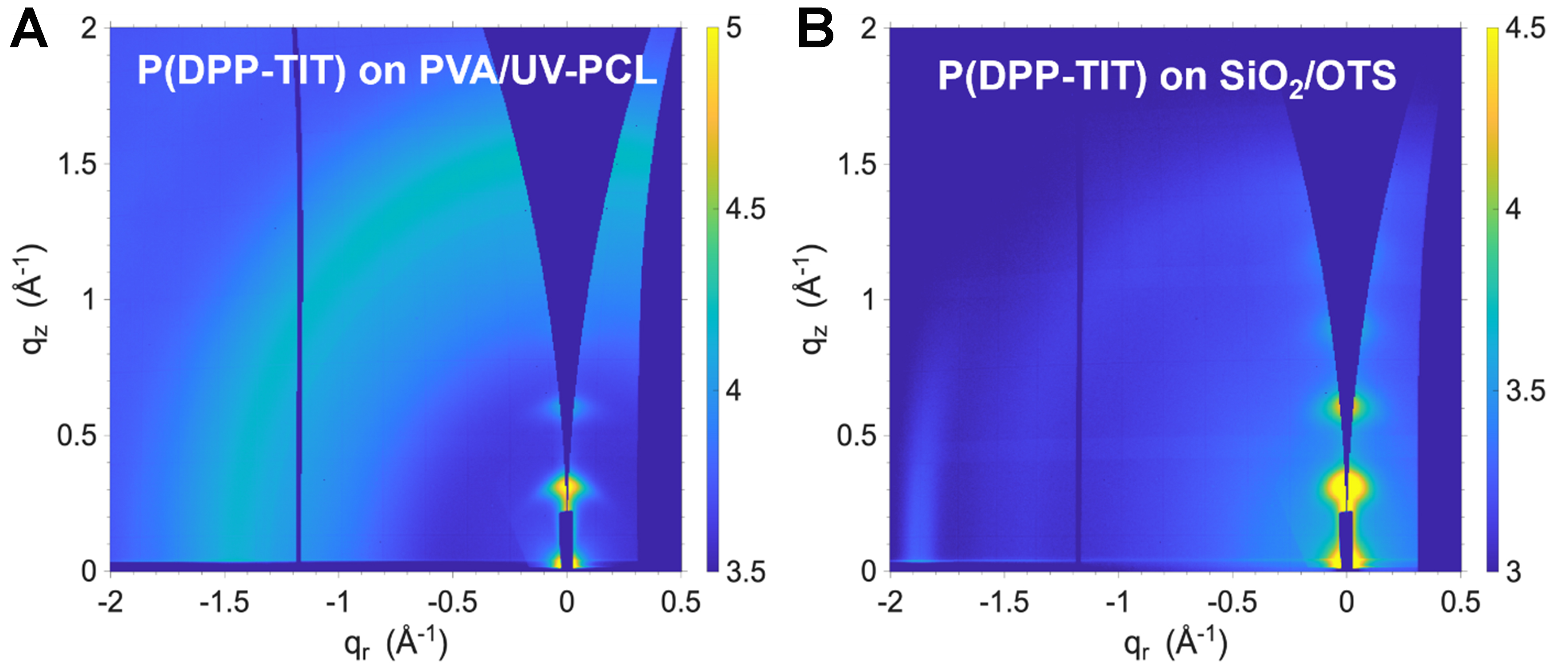
Figure 3. GIWAXS scattering patterns of DPP-imine conjugated polymer thin films deposited on (A) the bilayer dielectric (PVA/UV-PCL) and (B) on SiO2/OTS. GIWAXS: Grazing-incidence wide-angle X-ray scattering; DPP: diketopyrrolopyrrole; PVA: poly(vinyl alcohol); UV: ultraviolet; PCL: poly(caprolactone); OTS: octyltrichlorosilane; P(DPP-TIT): poly diketopyrrolopyrrole thiophene-imine-thiophene.
Stacking parameters and crystallization data of P(DPP-TIT) on OTS-SiO2 and degradable polymer substrates
| Dielectrics | Lamellar spacing | π-π spacing | FWHM [1/Å] | CCL [Å] | ||
| Peak position [1/Å] | d-d distance [Å] | Peak position [1/Å] | d-d distance [Å] | |||
| SiO2/OTS | 0.247 | 25.438 | 1.75 | 3.590 | 0.101 | 55.988 |
| PVA/UV-PCL | 0.255 | 24.640 | n/a | n/a | n/a | n/a |
Raman microscopy was employed to gain a deeper understanding of the morphology of P(DPP-TIT) on OTS-treated SiO2 and PVA/UV-PCL dielectric surface. This technique is highly sensitive to local polymer ordering, permitting subtle variations in conjugation length or miscibility within the material to be detected[81-84]. By tracking characteristic vibrational peaks specific to the DPP-based semiconductor, chemical or compositional maps can be generated. Figure 4A compares Raman spectra for OTFT with P(DPP-TIT) deposited on OTS-treated SiO2 and on PVA/UV-PCL. Distinct Raman features of the DPP-based semiconductor include the symmetric C=C stretching of the thiophene backbone at ~1,412 cm-1, symmetric C–N and C–C stretches associated with the DPP acceptor at ~1,365 cm-1, and asymmetric C=C stretching from the DPP and thiophene lactam rings at ~1,512 cm-1 [Figure 4A]. Figure 4B and C depict the Raman intensity maps for 19 × 19 µm2 of an OTFT device fabricated by depositing P(DPP-TIT) on OTS-treated SiO2 and on a degradable dielectric (PVA/UV-PCL), respectively. These figures demonstrate the normalized intensity value of the DPP-based semiconductor (at ~1,512 cm-1) and provide a visual representation of the chemical uniformity of the P(DPP-TIT) film to complement the Raman spectrum [Figure 4A]. Raman maps reveal that the intensity of P(DPP-TIT) on PVA/UV-PCL dielectric is relatively more uniform than when deposited on OTS-treated SiO2. A more packed and uniform structure of P(DPP-TIT) on a degradable dielectric surface can be attributed to fewer deep interfacial traps at the dielectric/semiconductor interface, enabling a more continuous conjugated network.
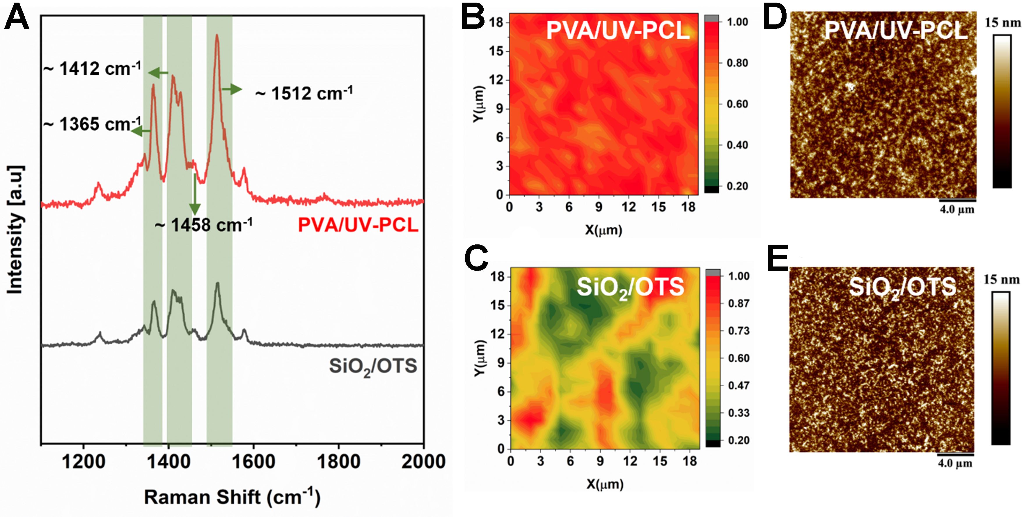
Figure 4. Raman spectra (A) and maps (19 × 19 µm2) (B and C) of degradable P(DPP-TIT) semiconductor on bilayer dielectric (PVA/UV-PCL) and OTS-treated SiO2. 20 × 20 μm AFM topography images of thin films of P(DPP-TIT) deposited on (D) the degradable polymer dielectric and (E) OTS-treated SiO2. P(DPP-TIT): Poly diketopyrrolopyrrole thiophene-imine-thiophene; PVA: poly(vinyl alcohol); UV: ultraviolet; PCL: poly(caprolactone); OTS: octyltrichlorosilane; AFM: atomic force microscopy.
The effect of the degradable polymer substrate and dielectric on the thin-film morphology was further characterized by AFM. Thin films were cast via spin-coating onto the bilayer dielectric (PVA/UV-PCL) [Figure 4D] and on OTS-treated SiO2 [Figure 4E] and were imaged over a 20 × 20 μm2 area to evaluate large-scale surface features. In both cases, P(DPP-TIT) exhibited morphological characteristics typical of DPP-based semiconductors, with uniform grain-like domains and no evidence of phase separation or aggregation[85,86]. The root-mean-square (RMS) roughness was 2.97 nm for the polymer substrate and
As depicted in Figure 1B, exposure of the fabricated OTFT to acidic medium (1 M HCl) for 7 days led to the degradation of P(DPP-TIT) layer and possibly the dissolution of bilayer dielectric layer based on PVA, while subsequent immersion of the degradable PLA substrate and patterned gold coated gate electrode in basic buffer solution (pH ~10) resulted in the gradual degradation of the PLA matrix in 20 days, leaving behind only dispersed gold micro and nanoparticles. This combination of structural design and sequential degradation demonstrates the feasibility of fabricating a high-performance yet transient OTFT system using biodegradable materials. UV-Vis spectroscopy was employed to track the degradation of imine groups in the P(DPP-TIT) polymers thin film [Figure 5]. The films were submerged in 1 M HCl at specified time intervals of 15 min, 30 min, and 1 h, upon which the spectral data was collected, as per Figure 5A. Progressive cleavage of the imine bonds results in the depolymerization of the material into oligomeric and monomeric species, which exhibit negligible absorption in the visible spectrum[18,36,43]. This can be observed in Figure 5B, by the progressive decrease in absorbance of the λ0-1 after just 15 min of submersion, as well as an observable widening hyperchromic shift, indicating polymer chain scission[16]. The absorbance continues to decrease more drastically after 30 min, and by 1 h, only approximately 20% of the initial λ0-1 absorbance remains, suggesting that the solid-state film of P(DPP-TIT) can undergo rapid depolymerization under aqueous acidic conditions. In comparison with previously established reports of the degradation of P(DPP-TIT) based thin films, this variant of P(DPP-TIT) has a degree of polymerization of 11 repeat units, and relatively narrow dispersity of 1.55, as per Supplementary Table 1. Both values are indicative that P(DPP-TIT) has a relatively low molecular weight, with polymer chains having relatively similar lengths[89]. The combination of these factors can provide faster degradation in comparison to previously established polymers possessing similar alkyl chains and conjugated backbones[43]. This is noteworthy, as literature reports indicate that polymers with reduced molecular weights degrade more readily, which complements the other components of the OTFT system that are also engineered for rapid breakdown[90,91]. Together, these design features ensure that the material maintains strong charge transport characteristics during operation while facilitating efficient degradation after use. Notably, as shown in Figure 5A, the π−π* transition peak centered at 450 nm associated with intrachain charge delocalization diminished at a slower rate in comparison to λ0-1 and λ0-0 absorbance peaks. The decay in absorbance of this peak is associated with the hydrolysis and subsequent ring-opening of the DPP motif[41]. With these observations, we hypothesize that in the solid state, the polymer undergoes chain scission via hydrolysis of the imine bonds within the conjugated backbone, which is then followed by destruction of the DPP motif itself[92].
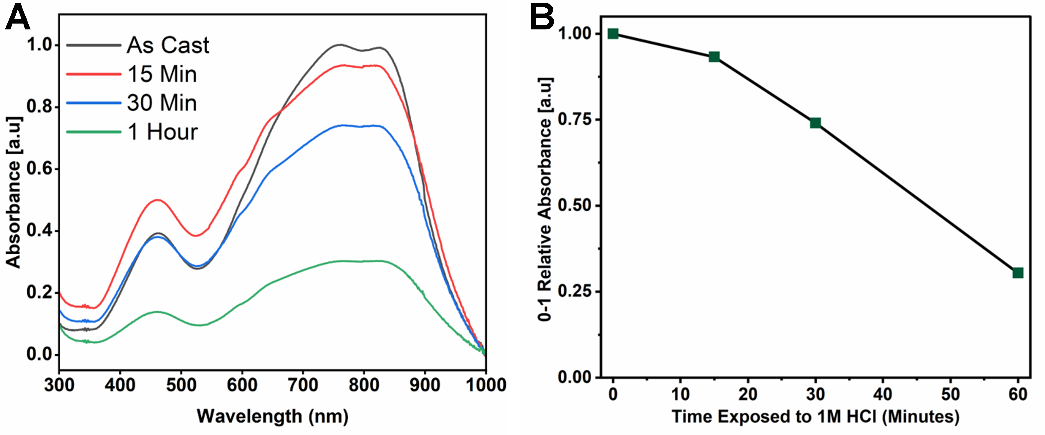
Figure 5. (A) UV-Vis spectra of the λ0-1-based normalized absorbance of P(DPP-TIT) thin films on quartz substrates upon submersion in aqueous 1 M HCl solution at selected time intervals; (B) Line plot of UV-Vis spectra quantifying the decrease in λ0-1 over a period of 1 h
We have also investigated the full device degradation and component recovery leveraging dual trigger dissolution: the imine-containing DPP-based semiconductor degrades under acidic conditions[43], while the PLA substrate dissolves in basic environments[24,93], enabling sequential separation and extraction of device layers. To demonstrate the degradation of the degradable P(DPP-TIT) semiconductor, a device was immersed in 1 M HCl solution and monitored for 7 days. Raman microscopy performed after exposure revealed the complete disappearance of the typical DPP polymer semiconductor peaks, as per Figure 6A, associated with the delocalized conjugated backbone alkene and aromatic spectral signatures. There was also a weak vibration peak observed at ~1,458 cm-1, which can be assigned to O-H and C-H bending for PVA film[94] [Figure 6A]. Hence, the disappearance of characteristic peaks of P(DPP-TIT) and PVA confirms that the active semiconductor layer was fully degraded along with full dissolution of the thin bilayer dielectric. Subsequently, the remaining layers (PLA substrate and gate electrode) were immersed in a basic buffer solution with a pH of ~10 to facilitate degradation. Raman measurements following this treatment displayed no characteristic peaks of PLA, yielding a flat baseline, which indicates that all the OTFT layers, including the P(DPP-TIT) semiconductor, substrate (PLA), and dielectric (PVA/UV-PCL), were completely degraded, leaving micro/nano particles of gold. The corresponding optical images shown in Figure 6B-D depict the stepwise degradation process of the OTFT device in an acidic and basic medium. Figure 6B shows the intact device prior to immersion. Figure 6C demonstrates the complete degradation of the active semiconducting layer and dissolution of PVA and UV-PCL (monolayer), along with the visible disintegration of the source and drain electrodes during immersion. Finally, Figure 6D reveals the presence of only gold micro/nanoparticles remaining after the complete degradation of the substrate in basic buffer solution of NaOH (pH ~10). Similarly, Figures 6E-G illustrate the degradation sequence for the free-standing OTFT structure. Figure 6E shows an OTFT device before it was immersed in 1 M HCl, Figure 6F displays the free-standing PLA layer with the remaining gate electrode pattern, and Figure 6G shows a free-standing gold particle following substrate degradation. Overall, these results and images clearly demonstrate a tiered degradation approach which enables separation of components and will facilitate separation, recovery and repurposing of the OTFT components.
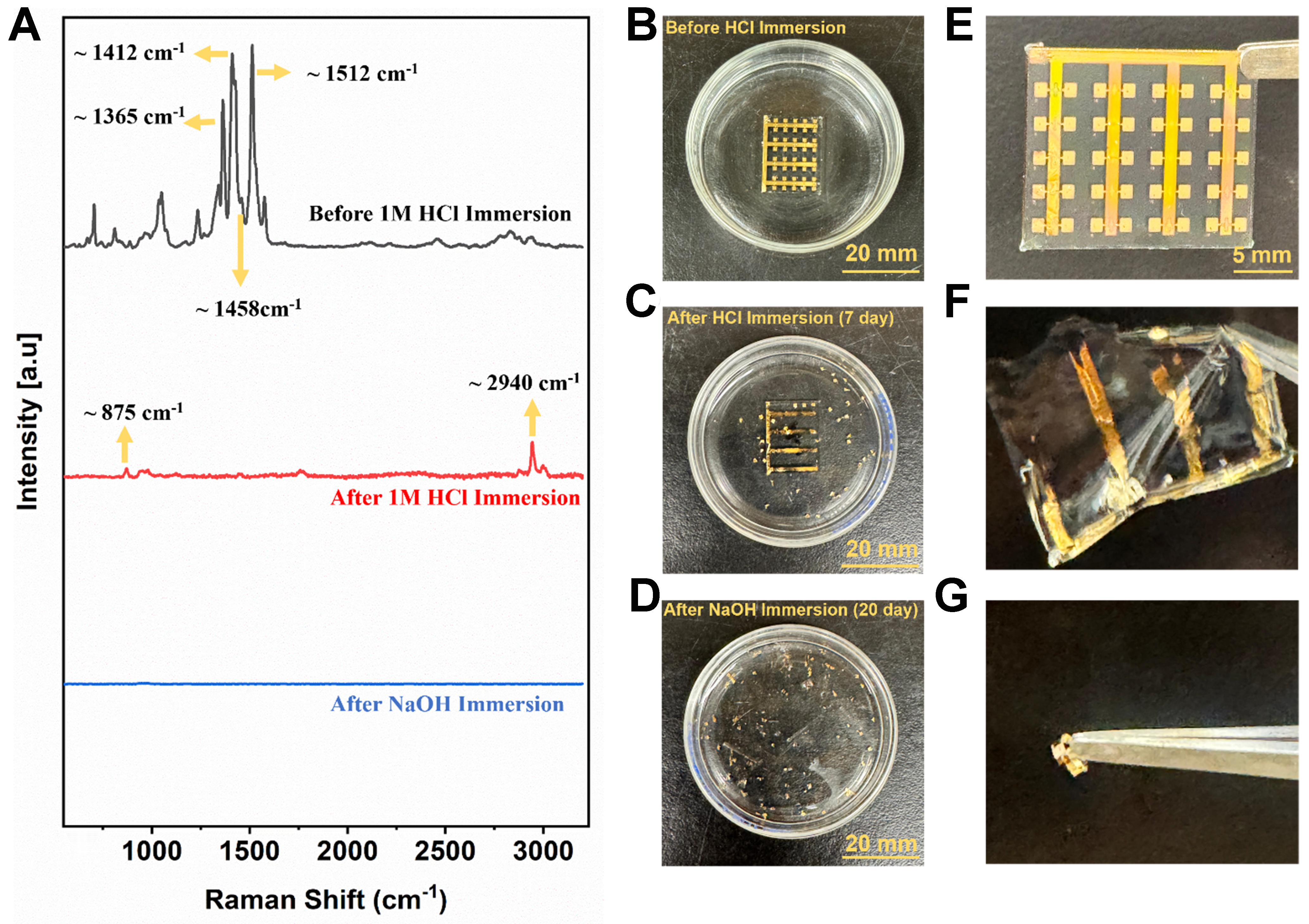
Figure 6. (A) Raman spectrum of the degradable OTFT device at different stages of degradation; (B-D) Photos of OTFTs before the immersion in 1 M HCl, after immersion in 1 M HCl, and after the immersion in basic buffer solution (pH ~10), respectively; (E-G) Free-standing images of OTFT before the immersion in 1 M HCl, after immersion in 1 M HCl, and after the immersion in basic buffer solution, respectively. OTFT: Organic thin-film transistor.
Furthermore, the acid and base media employed in this work for the demonstration of sequential degradation are not intended to represent physiological or typical environmental conditions. Instead, they serve as accelerated conditions used to demonstrate selective layer removal and identify relative material stability within experimentally accessible time scales[37,93,95-97]. In potential industrial recovery or recycling scenarios, similar acceleration could be achieved through elevated temperatures and controlled pH to facilitate efficient material separation. Un-der natural environmental conditions, degradation would instead proceed more gradually through hydrolytic, enzymatic, or environmentally assisted processes. Over time, the material breaks into soluble fragments, supporting separation and reducing long-term persistence. Ac-cordingly, the presented strategy demonstrates the feasibility of controlled disassembly while recognizing that degradation in real-world environments would occur at slower rates than those observed under accelerated laboratory conditions.
CONCLUSION
In summary, biocompatible and fully biodegradable OTFTs were prepared using an imine-based degradable semiconducting polymer P(DPP-TIT), coupled with a biodegradable substrate (PLA) and dielectric (PVA/UV-PCL). The use of a bilayer gate dielectric effectively reduced the VT of P(DPP-TIT)-based p-type OTFTs from -16.1 to -2 V while maintaining electrical performance comparable to OTFTs employing conventional SiO2 dielectrics. Raman spectroscopy/microscopy, GIWAXS, and AFM analyses revealed similar morphological and structural characteristics consistent with the observed device performance. Finally, we demonstrated the stepwise degradation of each device layer under acidic and basic environments, confirming the complete disintegration of the OTFT components. This work highlights a promising approach toward sustainable, transient electronics that combine reliable functionality with environmental degradability.
DECLARATIONS
Acknowledgments
We acknowledge SOLEIL for beamtime provision on the beamline SIRIUS. We also thank Laura E. Dickson for her assistance in analyzing GIWAX results.
Authors’ contributions
Conducted the experimental work including device fabrication, degradation experiments, data analysis, and wrote the initial draft of the manuscript: Ali, M.
Synthesized the semiconducting polymer, conducted UV-Vis, and assisted in data analysis and editing of the manuscript: Nyayachavadi, A.
Conducted experiments and assisted in data analysis: Pascual, S. G.
Performed numerical simulation analysis: Park, J.
Analysed numerical simulation data and edited the manuscript: Kim, C. H.
Performed the GIWAXS and collected the data: Hemmerle, A.
Helped design and created schematic figures and edited the manuscript: Manion, J. G.
Acquired funding, managed supervision, directed the study, and assisted in writing and editing the manuscript: Lessard, B. H.
The manuscript was written through the contributions of all authors. All authors have given approval to the final version of the manuscript.
Availability of data and materials
The data supporting the findings of this study are available in the article and its Supplementary Materials. All other reasonable requests can be directed to the corresponding author.
AI and AI-assisted tools statement
Not applicable.
Financial support and sponsorship
This work was supported by Natural Sciences and Engineering Research Council of Canada (NSERC) Discovery program (RGPIN-2025-03936 to Lessard, B. H.). We thank the Ontario Research Fund (Large Infrastructure Fund) and Canadian Foundation for Innovation, CFI# 40178 (HIIT) and CFI# 43247 (SSMART), for support in the acquisition and maintenance of the infrastructure needed for this project. We also thank SOLEIL for beamtime under the proposal 99250162.
Conflicts of interest
All authors declared that there are no conflicts of interest.
Ethical approval and consent to participate
Not applicable.
Consent for publication
Not applicable.
Copyright
© The Author(s) 2026.
Supplementary Materials
REFERENCES
1. Kang, S.; Yin, L.; Bettinger, C. The emergence of transient electronic devices. MRS. Bull. 2020, 45, 87-95.
2. Fu, K. K.; Wang, Z.; Dai, J.; Carter, M.; Hu, L. Transient electronics: materials and devices. Chem. Mater. 2016, 28, 3527-39.
3. Chiong, J. A.; Tran, H.; Lin, Y.; Zheng, Y.; Bao, Z. Integrating emerging polymer chemistries for the advancement of recyclable, biodegradable, and biocompatible electronics. Adv. Sci. 2021, 8, e2101233.
4. Tan, M. J.; Owh, C.; Chee, P. L.; Kyaw, A. K. K.; Kai, D.; Loh, X. J. Biodegradable electronics: cornerstone for sustainable electronics and transient applications. J. Mater. Chem. C. 2016, 4, 5531-58.
5. Chen, G.; Xu, L.; Zhang, P.; et al. Seawater degradable triboelectric nanogenerators for blue energy. Adv. Mater. Technol. 2020, 5, 2000455.
6. Hwang, S. W.; Tao, H.; Kim, D. H.; et al. A physically transient form of silicon electronics. Science 2012, 337, 1640-4.
7. Gao, Y.; Zhang, Y.; Wang, X.; et al. Moisture-triggered physically transient electronics. Sci. Adv. 2017, 3, e1701222.
8. Loi, M. A.; da Como, E.; Dinelli, F.; et al. Supramolecular organization in ultra-thin films of α-sexithiophene on silicon dioxide. Nat. Mater. 2005, 4, 81-5.
9. Kaltenbrunner, M.; Sekitani, T.; Reeder, J.; et al. An ultra-lightweight design for imperceptible plastic electronics. Nature 2013, 499, 458-63.
10. Sekitani, T.; Nakajima, H.; Maeda, H.; et al. Stretchable active-matrix organic light-emitting diode display using printable elastic conductors. Nat. Mater. 2009, 8, 494-9.
11. Tee, B. C. K.; Chortos, A.; Berndt, A.; et al. A skin-inspired organic digital mechanoreceptor. Science 2015, 350, 313-6.
12. Klauk, H.; Zschieschang, U.; Pflaum, J.; Halik, M. Ultralow-power organic complementary circuits. Nature 2007, 445, 745-8.
13. Henson, Z. B.; Müllen, K.; Bazan, G. C. Design strategies for organic semiconductors beyond the molecular formula. Nat. Chem. 2012, 4, 699-704.
14. Li, R.; Wang, L.; Kong, D.; Yin, L. Recent progress on biodegradable materials and transient electronics. Bioact. Mater. 2018, 3, 322-33.
15. La Mattina, A. A.; Mariani, S.; Barillaro, G. Bioresorbable materials on the rise: from electronic components and physical sensors to in vivo monitoring systems. Adv. Sci. 2020, 7, 1902872.
16. Feig, V. R.; Tran, H.; Bao, Z. Biodegradable polymeric materials in degradable electronic devices. ACS. Cent. Sci. 2018, 4, 337-48.
17. Irimia-Vladu, M. “Green” electronics: biodegradable and biocompatible materials and devices for sustainable future. Chem. Soc. Rev. 2014, 43, 588-610.
18. Lei, T.; Guan, M.; Liu, J.; et al. Biocompatible and totally disintegrable semiconducting polymer for ultrathin and ultralightweight transient electronics. Proc. Natl. Acad. Sci. U. S. A. 2017, 114, 5107-12.
19. Bettinger, C. J.; Bao, Z. Organic thin-film transistors fabricated on resorbable biomaterial substrates. Adv. Mater. 2010, 22, 651-5.
20. Reichert, C. L.; Bugnicourt, E.; Coltelli, M. B.; et al. Bio-based packaging: materials, modifications, industrial applications and sustainability. Polymers 2020, 12, 1558.
21. Chiellini, E.; Corti, A.; D’Antone, S.; Solaro, R. Biodegradation of poly (vinyl alcohol) based materials. Prog. Polym. Sci. 2003, 28, 963-1014.
22. Van Etten, E. A.; Ximenes, E. S.; Tarasconi, L. T.; Garcia, I. T.; Forte, M. M.; Boudinov, H. Insulating characteristics of polyvinyl alcohol for integrated electronics. Thin. Solid. Films. 2014, 568, 111-6.
23. Tran, H.; Feig, V. R.; Liu, K.; Zheng, Y.; Bao, Z. Polymer chemistries underpinning materials for skin-inspired electronics. Macromolecules 2019, 52, 3965-74.
24. Ali, M.; Ronnasi, B.; Ourabi, M.; et al. Cytocompatible, disintegrable, low-voltage operation n-type organic thin film transistors. Mater. Adv. 2025, 6, 557-68.
25. Jin, S. H.; Yu, J. S.; Kim, J. W.; et al. 34.2: PMMA Buffer‐Layer Effects on Electrical Performance of Pentacene OTFTs with a Cross‐linked PVA Gate Insulator on a Flexible Substrate. Symp. Digest. of. Tech. Papers. 2003, 34, 1088-91.
26. Jin, S. H.; Yu, J. S.; Lee, C. A.; Kim, J. W.; Park, B. G.; Lee, J. D. Pentacene OTFTs with PVA gate insulators on a flexible substrate. J. Korean. Phys. Soc. 2004, 44, 181-4. https://khu.elsevierpure.com/en/publications/pentacene-otfts-with-pva-gate-insulators-on-a-flexible-substrate/. (accessed 2026-05-15).
27. Tousignant, M. N.; Lin, Z. S.; Brusso, J.; Lessard, B. H. Interfacial ultraviolet cross-linking of green bilayer dielectrics. ACS. Appl. Mater. Interfaces. 2023, 15, 3680-8.
28. Tousignant, M. N.; Ronnasi, B.; Tischler, V.; Lessard, B. H. N‐type single walled carbon nanotube thin film transistors using green tri‐layer polymer dielectric. Adv. Mater. Inter. 2023, 10, 2300079.
29. Rullyani, C.; Ramesh, M.; Sung, C.; Lin, H.; Chu, C. Natural polymers for disposable organic thin film transistors. Org. Electron. 2018, 54, 154-60.
30. She, X.; Liu, J.; Zhang, J.; Gao, X.; Wang, S. Spatial profile of charge storage in organic field-effect transistor nonvolatile memory using polymer electret. Appl. Phys. Lett. 2013, 103, 143302.
31. Chan, E. W. C.; Sun, X.; Travas-Sejdic, J. Recent progress and future prospects in transient polymer electronics. Macromolecules 2023, 56, 3755-73.
32. Liu B. Recent advances in biodegradable conducting polymers and their biomedical applications. Biomacromolecules 2018, 19, 1783-803.
33. Guimard, N. K.; Sessler, J. L.; Schmidt, C. E. Towards a biocompatible, biodegradable copolymer incorporating electroactive oligothiophene units. Macromolecules 2009, 42, 502-11.
34. Guo, B.; Finne-Wistrand, A.; Albertsson, A. Enhanced electrical conductivity by macromolecular architecture: hyperbranched electroactive and degradable block copolymers based on poly(ε-caprolactone) and aniline pentamer. Macromolecules 2010, 43, 4472-80.
35. Chakraborty, D.; Plajer, A. J. Recent advances in polyimine chemistry: synthesis, functional design, and degradation. J. Polym. Sci. 2025, 63, 4383-93.
36. Uva, A.; Kim, Y.; Michailovich, S.; et al. Impact of imine bonds on the electronic properties of degradable carotenoid-based conjugated polymers. Polym. Chem. 2025, 16, 2817-28.
37. Tran, H.; Nikzad, S.; Chiong, J. A.; et al. Modular synthesis of fully degradable imine-based semiconducting p-type and n-type polymers. Chem. Mater. 2021, 33, 7465-74.
38. Zade, S. S.; Zamoshchik, N.; Bendikov, M. From short conjugated oligomers to conjugated polymers. Lessons from studies on long conjugated oligomers. Acc. Chem. Res. 2011, 44, 14-24.
39. Hsu, N. S. Y.; Lin, A.; Uva, A.; Huang, S. H.; Tran, H. Direct arylation polymerization of degradable imine-based conjugated polymers. Macromolecules 2023, 56, 8947-55.
40. Kotewicz, K.; Franco, L. R.; Araujo, M.; Wang, E. Acidochromic behaviors of indacenodithiophene-based conjugated polymers containing azo, imine, and vinyl bonds. Macromolecules 2025, 58, 2719-29.
41. David, J.; Weiter, M.; Vala, M.; Vyňuchal, J.; Kučerík, J. Stability and structural aspects of diketopyrrolopyrrole pigment and its N-alkyl derivatives. Dyes. Pigm. 2011, 89, 137-43.
42. Liu, Q.; Bottle, S. E.; Sonar, P. Developments of diketopyrrolopyrrole-dye-based organic semiconductors for a wide range of applications in electronics. Adv. Mater. 2020, 32, e1903882.
43. Chiong, J. A.; Zheng, Y.; Zhang, S.; et al. Impact of molecular design on degradation lifetimes of degradable imine-based semiconducting polymers. J. Am. Chem. Soc. 2022, 144, 3717-26.
44. Mei, J.; Bao, Z. Side chain engineering in solution-processable conjugated polymers. Chem. Mater. 2014, 26, 604-15.
45. Yang, Y.; Liu, Z.; Zhang, G.; Zhang, X.; Zhang, D. The effects of side chains on the charge mobilities and functionalities of semiconducting conjugated polymers beyond solubilities. Adv. Mater. 2019, 31, e1903104.
46. Mooney, M.; Nyayachavadi, A.; Rondeau-Gagné, S. Eco-friendly semiconducting polymers: from greener synthesis to greener processability. J. Mater. Chem. C. 2020, 8, 14645-64.
47. Voskerician, G.; Shawgo, R. S.; Hiltner, P. A.; Anderson, J. M.; Cima, M. J.; Langer, R. In vivo inflammatory and wound healing effects of gold electrode voltammetry for MEMS micro-reservoir drug delivery device. IEEE. Trans. Biomed. Eng. 2004, 51, 627-35.
48. Wilson, G. S.; Hu, Y. Enzyme-based biosensors for in vivo measurements. Chem. Rev. 2000, 100, 2693-704.
49. Peng, M.; Wang, J.; Li, Z.; et al. Three-dimensional flexible and stretchable gold foam scaffold for real-time electrochemical sensing in cells and in vivo. Talanta 2023, 253, 123891.
50. Edelman, E. R.; Seifert, P.; Groothuis, A.; Morss, A.; Bornstein, D.; Rogers, C. Gold-coated NIR stents in porcine coronary arteries. Circulation 2001, 103, 429-34.
51. Voskerician, G.; Shive, M. S.; Shawgo, R. S.; et al. Biocompatibility and biofouling of MEMS drug delivery devices. Biomaterials 2003, 24, 1959-67.
52. Ali, M.; Ewenike, R. B.; Manion, J. G.; Lessard, B. H. Two is better than one: how the addition of multiple biodegradable polymers can improve organic thin-film transistor performance. ACS. Appl. Mater. Interfaces. 2025, 17, 1734-42.
53. Manion, J.; Lessard, B. H. High-throughput characterization is key to report reliable organic thin-film transistor performance. Nat. Rev. Mater. 2024, 9, 377-8.
54. Hemmerle, A.; Aubert, N.; Moreno, T.; et al. Opportunities and new developments for the study of surfaces and interfaces in soft condensed matter at the SIRIUS beamline of Synchrotron SOLEIL. J. Synchrotron. Radiat. 2024, 31, 162-76.
55. Jiang, Z. GIXSGUI : a MATLAB toolbox for grazing-incidence X-ray scattering data visualization and reduction, and indexing of buried three-dimensional periodic nanostructured films. J. Appl. Crystallogr. 2015, 48, 917-26.
56. Carvalho, J. R. G.; Conde, G.; Antonioli, M. L.; et al. Biocompatibility and biodegradation of poly(lactic acid) (PLA) and an immiscible PLA/poly(ε-caprolactone) (PCL) blend compatibilized by poly(ε-caprolactone-b-tetrahydrofuran) implanted in horses. Polym. J. 2020, 52, 629-43.
57. Silva, C.; Thomazini, D.; Pinheiro, A.; et al. Collagen–hydroxyapatite films: piezoelectric properties. Mater. Sci. Eng. B. 2001, 86, 210-8.
58. Ponce Ortiz, R.; Facchetti, A.; Marks, T. J. High-k organic, inorganic, and hybrid dielectrics for low-voltage organic field-effect transistors. Chem. Rev. 2010, 110, 205-39.
59. Amin, E. M.; Karmakar, N. C.; Winther-Jensen, B. Polyvinyl-alcohol (PVA)-based RF humidity sensor in microwave frequency. PIER. B. 2013, 54, 149-66.
60. Tsai, T.; Chang, J.; Wen, T.; Guo, T. Manipulating the hysteresis in poly(vinyl alcohol)‐dielectric organic field‐effect transistors toward memory elements. Adv. Funct. Mater. 2013, 23, 4206-14.
61. Tousignant, M. N.; Rice, N. A.; Peltekoff, A.; et al. Improving thin-film properties of poly(vinyl alcohol) by the addition of low-weight percentages of cellulose nanocrystals. Langmuir 2020, 36, 3550-7.
62. Suresh Babu, K. V.; Rama Teja, A. S.; Srinivas Babu, N.; Arunachalam, V.; Maheswar, C. V. S.; Audisesha Reddy, K. Methods of decontamination of toluene di-isocyanate (TDI) spills and leftovers. Res. J. Chem. Sci. 2014, 4, 89-93. https://isca.me/rjcs/Archives/v4/i4/13.ISCA-RJCS-2014-039.pdf. (accessed 2026-05-18).
63. Tousignant, M. N.; Rice, N. A.; Niskanen, J.; et al. High performance organic electronic devices based on a green hybrid dielectric. Adv. Elect. Mater. 2021, 7, 2100700.
64. Grau, G.; Subramanian, V. Dimensional scaling of high-speed printed organic transistors enabling high-frequency operation. Flex. Print. Electron. 2020, 5, 014013.
65. Khan, Y.; Thielens, A.; Muin, S.; Ting, J.; Baumbauer, C.; Arias, A. C. A new frontier of printed electronics: flexible hybrid electronics. Adv. Mater. 2020, 32, e1905279.
66. Subbarao, N. V.; Mandal, S.; Gedda, M.; Iyer, P. K.; Goswami, D. K. Effect of temperature on hysteresis of dipolar dielectric layer based organic field-effect transistors: a temperature sensing mechanism. Sens. Actuators. A. Phys. 2018, 269, 491-9.
67. Brixi, S.; Radford, C. L.; Tousignant, M. N.; et al. Poly(ionic liquid) gating materials for high-performance organic thin-film transistors: the role of block copolymer self-assembly at the semiconductor interface. ACS. Appl. Mater. Interfaces. 2022, 14, 40361-70.
68. Hadidi, M.; Jafarzadeh, S.; Forough, M.; et al. Plant protein-based food packaging films; recent advances in fabrication, characterization, and applications. Trends. Food. Sci. Technol. 2022, 120, 154-73.
69. Zhang, H.; Zhang, F.; Sun, J.; et al. Solution-processed organic field-effect transistors with cross-linked poly(4-vinylphenol)/polyvinyl alcohol bilayer dielectrics. Appl. Surf. Sci. 2019, 478, 699-707.
70. Nawaz, A.; Hümmelgen, I. A. Poly(vinyl alcohol) gate dielectric in organic field-effect transistors. J. Mater. Sci. Mater. Electron. 2019, 30, 5299-326.
71. Sun, Y.; Liu, Y.; Wang, Y.; Di, C.; Wu, W.; Yu, G. Polymer gate dielectrics with self-assembled monolayers for high-mobility organic thin-film transistors based on copper phthalocyanine. Appl. Phys. A. 2009, 95, 777-80.
72. Puigdollers, J.; Voz, C.; Fonrodona, M.; et al. Copper phthalocyanine thin-film transistors with polymeric gate dielectric. J. Non. Cryst. Solids. 2006, 352, 1778-82.
73. Vasimalla, S.; Subbarao, N. V. V.; Gedda, M.; Goswami, D. K.; Iyer, P. K. Effects of dielectric material, HMDS layer, and channel length on the performance of the perylenediimide-based organic field-effect transistors. ACS. Omega. 2017, 2, 2552-60.
74. Park, J.; Kim, S.; Bae, J.; et al. Inseparability between charge-injection barrier and out-of-plane mobility in staggered thin-film transistors. Appl. Phys. Lett. 2025, 127, 113503.
75. Lee, H.; Lim, K.; Kim, C. Vertical organic transistors with a permeable base: from fundamentals to performance prediction. J. Mater. Chem. C. 2023, 11, 5422-30.
76. Bae, J.; Park, S.; Jung, H.; Ko, E.; Kymissis, I.; Kim, C. Polymer field-effect transistors with inkjet-printed silver electrodes: from device fabrication to circuit simulation. J. Mater. Sci. Mater. Electron. 2024, 35, 11819.
77. Kim, Y. E.; Jung, H.; Park, J. H.; Yoo, H.; Kim, C. Energy gap and orbital mixing in DNTT/PTCDI-C8 heterostructure. Org. Electron. 2025, 138, 107195.
78. Lee, H.; Kim, Y. E.; Bae, J.; Jung, S.; Sporea, R. A.; Kim, C. H. High-performance organic source-gated transistors enabled by the indium-tin oxide-diketopyrrolopyrrole polymer interface. ACS. Appl. Mater. Interfaces. 2023, 15, 10918-25.
79. Müller, C.; Aghamohammadi, M.; Himmelberger, S.; et al. One‐step macroscopic alignment of conjugated polymer systems by epitaxial crystallization during spin‐coating. Adv. Funct. Mater. 2013, 23, 2368-77.
80. Schulz, G. L.; Ludwigs, S. Controlled crystallization of conjugated polymer films from solution and solvent vapor for polymer electronics. Adv. Funct. Mater. 2017, 27, 1603083.
81. Yu, S. H.; Park, K. H.; Kim, Y.; Chung, D. S.; Kwon, S. Fine molecular tuning of diketopyrrolopyrrole-based polymer semiconductors for efficient charge transport: effects of intramolecular conjugation structure. Macromolecules 2017, 50, 4227-34.
82. Mukhopadhyay, T.; Puttaraju, B.; Roy, P.; et al. Facile synthesis and chain-length dependence of the optical and structural properties of diketopyrrolopyrrole-based oligomers. Chemistry 2017, 23, 13718-23.
83. McPherson, T. E. Characterizing the morphology of solvent annealed PCBM/P3HT bilayers using GIXRD and Raman spectroscopy. 2014. https://trace.tennessee.edu/utk_gradthes/2735/. (accessed 2026-05-18).
84. Cranston, R. R.; Lanosky, T. D.; Ewenike, R.; Mckillop, S.; King, B.; Lessard, B. H. Polarized Raman microscopy to image microstructure changes in silicon phthalocyanine thin-films. Small. Sci. 2024, 4, 2300350.
85. Gao, Y.; Bai, J.; Sui, Y.; et al. High mobility ambipolar diketopyrrolopyrrole-based conjugated polymers synthesized via direct arylation polycondensation: influence of thiophene moieties and side chains. Macromolecules 2018, 51, 8752-60.
86. Opoku, H.; Nketia-Yawson, B.; Shin, E.; Noh, Y. Organic field-effect transistors processed by an environmentally friendly non-halogenated solvent blend. J. Mater. Chem. C. 2018, 6, 661-7.
87. Kim, M.; Ryu, S. U.; Park, S. A.; et al. Donor–acceptor‐conjugated polymer for high‐performance organic field‐effect transistors: a progress report. Adv. Funct. Mater. 2020, 30, 1904545.
88. Ma, H.; Yip, H.; Huang, F.; Jen, A. K. Interface engineering for organic electronics. Adv. Funct. Mater. 2010, 20, 1371-88.
89. Hendsbee, A. D.; Li, Y. Performance comparisons of polymer semiconductors synthesized by direct (hetero)arylation polymerization (DHAP) and conventional methods for organic thin film transistors and organic photovoltaics. Molecules 2018, 23, 1255.
90. Charland-Martin, A.; Collier, G. S. Understanding degradation dynamics of azomethine-containing conjugated polymers. Macromolecules 2024, 57, 6146-55.
91. Sims, M. B.; Patel, K. Y.; Bhatta, M.; Mukherjee, S.; Sumerlin, B. S. Harnessing imine diversity to tune hyperbranched polymer degradation. Macromolecules 2018, 51, 356-63.
92. Jin, H.; Kim, K.; Park, S.; et al. Chemically recyclable conjugated polymer and one‐shot preparation of thermally stable and efficient bulk‐heterojunction from recycled monomer. Adv. Funct. Mater. 2023, 33, 2304930.
93. Ali, M.; Hoseyni, S. M.; Das, R.; Awais, M.; Basdogan, I.; Beker, L. A flexible and biodegradable piezoelectric‐based wearable sensor for non‐invasive monitoring of dynamic human motions and physiological signals. Adv. Mater. Technol. 2023, 8, 2300347.
94. Martinelli, A.; Matic, A.; Jacobsson, P.; et al. Structural analysis of PVA-based proton conducting membranes. Solid. State. Ionics. 2006, 177, 2431-5.
95. Curry, E. J.; Ke, K.; Chorsi, M. T.; et al. Biodegradable piezoelectric force sensor. Proc. Natl. Acad. Sci. U. S. A. 2018, 115, 909-14.
96. Bathaei, M. J.; Singh, R.; Mirzajani, H.; et al. Photolithography‐based microfabrication of biodegradable flexible and stretchable sensors. Adv. Mater. 2023, 35, e2207081.
Cite This Article
How to Cite
Download Citation
Export Citation File:
Type of Import
Tips on Downloading Citation
Citation Manager File Format
Type of Import
Direct Import: When the Direct Import option is selected (the default state), a dialogue box will give you the option to Save or Open the downloaded citation data. Choosing Open will either launch your citation manager or give you a choice of applications with which to use the metadata. The Save option saves the file locally for later use.
Indirect Import: When the Indirect Import option is selected, the metadata is displayed and may be copied and pasted as needed.
About This Article
Copyright

Data & Comments
Data
0


Comments
Comments must be written in English. Spam, offensive content, impersonation, and private information will not be permitted. If any comment is reported and identified as inappropriate content by OAE staff, the comment will be removed without notice. If you have any queries or need any help, please contact us at support@oaepublish.com.