



fig3
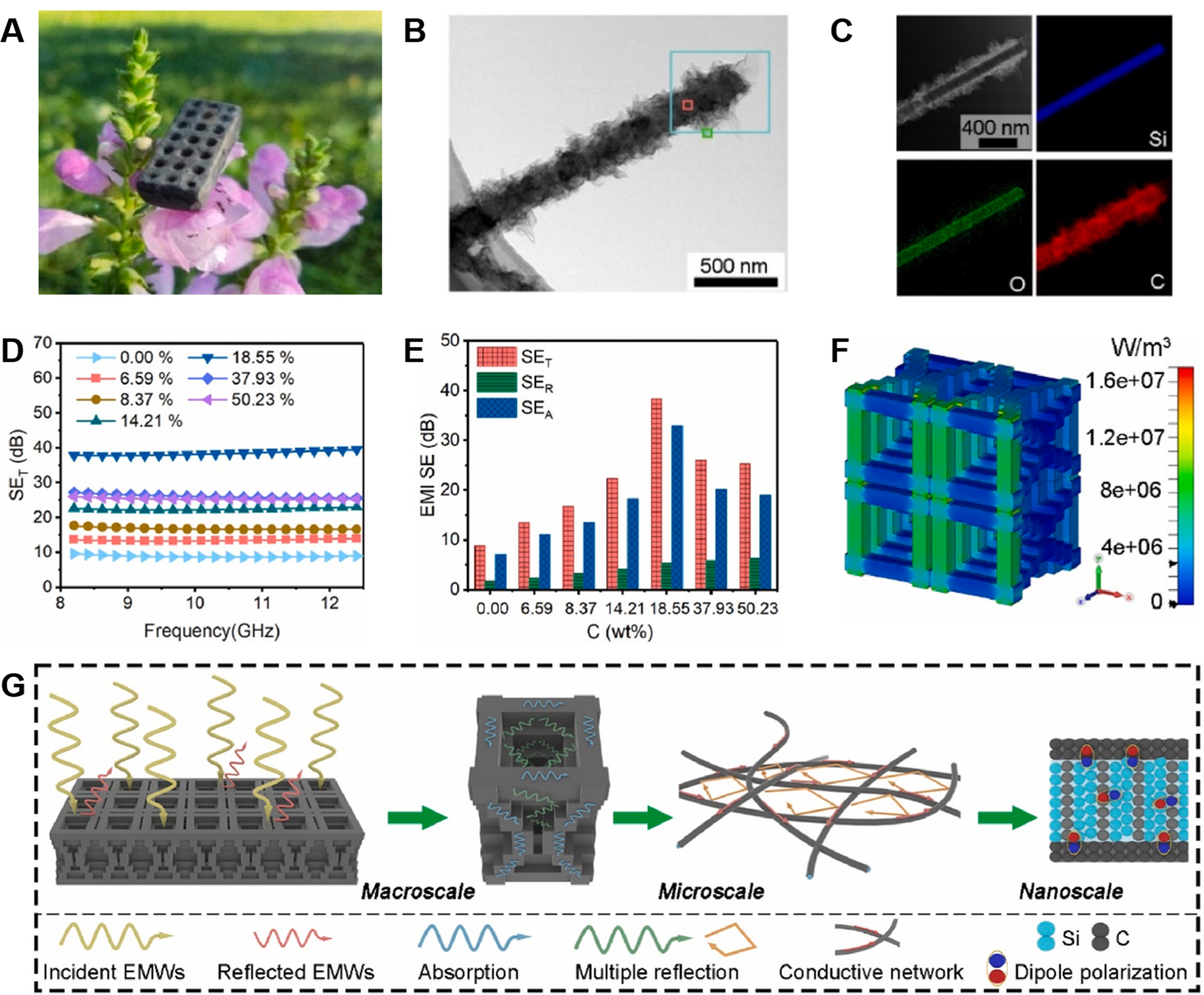
Figure 3. Robust SiC@C nanowire aerogel metastructures for EMI attenuation: (A) Optical image of the ultralight metastructure aerogel; (B) TEM image of an individual SiC@C nanowire; (C) HAADF-STEM micrograph with EDS elemental distribution maps; (D) Total EMI SE (SE_T) of metastructure aerogels at varying carbon contents; (E) SE_T, SE_R, and SE_A vs. carbon content; (F) Simulated power loss density distribution of the metastructure; (G) Multi-scale EMI attenuation mechanism from macroscale to nanoscale. (A-G) are reprinted with permission from Ref.[60]. © 2024 Elsevier. EMI: Electromagnetic interference; TEM: transmission electron microscopy; HAADF-STEM: high-angle annular dark-field scanning transmission electron microscopy; EDS: energy-dispersive X-ray spectroscopy; EMWs: electromagnetic waves.